Interfacial heat transport in two-dimensional heterostructures: From formation to functionality
Yufeng Zhang
Aoran Fan

Weigang Ma
Xing Zhang
*
*Correspondence to:
Xing Zhang, Key Laboratory for Thermal Science and Power Engineering of Ministry of Education, Department of Engineering Mechanics, Tsinghua University, Beijing 100084, China.
E-mail: x-zhang@tsinghua.edu.cn
Thermo-X. 2026;2:202620. 10.70401/tx.2026.0021
Received: May 14, 2026Accepted: June 23, 2026Published: June 23, 2026
Abstract
Two-dimensional (2D) heterostructures provide an unusually versatile platform for engineering interfaces at the atomic scale. As these materials move toward electronic, optoelectronic and multifunctional devices, heat flow across their interfaces is emerging as a central factor that governs performance, stability and reliability. Interfacial thermal transport has traditionally been treated as a material-pair-specific conductance that should be measured and optimized. In 2D heterostructures, however, the interface is not a passive boundary with a fixed thermal response. Its conductance is shaped by the structural history, local configuration and dynamic state of the interface. In this perspective, we discuss how interface formation, thermal metrology and microscopic phonon mechanisms together define heat flow across atomically thin heterointerfaces. We highlight how direct growth and transfer assembly create distinct opportunities for lateral and vertical interfaces, how Raman thermometry, pump-probe thermoreflectance and electrical methods quantify interfacial transport, and how elastic transmission, inelastic scattering and interface-specific vibrational states govern nanoscale heat flow. We then consider how intrinsic and external control of 2D heterointerfaces can be used to tune conductance for heat dissipation, local heat confinement, rectification and thermal switching. We argue that the future of the field lies in moving from passive characterization of interfacial thermal conductance toward predictive, spatially resolved and actively controlled heat flow in 2D heterostructures.
Graphical Abstract
Keywords
Two-dimensional heterostructures, interfacial thermal transport, phonon transport, thermal modulation, thermal functionality
1. Introduction
Two-dimensional (2D) heterostructures have reshaped the way interfaces are designed in condensed-matter systems. By stacking or stitching atomically thin crystals with distinct electronic structures and lattice symmetries, they create artificial materials in which charge, excitons, photons and lattice vibrations can be reorganized at the atomic scale[1-3]. This interfacial freedom has enabled phenomena ranging from interlayer charge transfer and moiré reconstruction to tunnelling, correlated electronic phases and polar switching[4-8]. As these systems move from model platforms toward electronic, optoelectronic and multifunctional architectures, the same interfaces that generate new physical behavior also become decisive pathways for heat flow[9,10].
Thermal transport across 2D heterointerfaces has traditionally been described by interfacial thermal conductance (ITC), a parameter that quantifies how efficiently heat crosses a boundary between two materials[11,12]. This description has been essential for analyzing atomically thin stacks, where heat generated by electrical bias, photoexcitation, carrier relaxation or local switching often encounters a sequence of van der Waals (vdW) gaps, lateral junctions, encapsulation layers and supporting substrates before it can be dissipated. In this conventional view, the interface is treated primarily as a thermal bottleneck whose conductance should be measured, modelled and increased.
However, 2D heterointerfaces offer a broader opportunity than this bottleneck picture suggests. Their thermal response is not determined solely by material identity, but by the local structure and state of the interface created during growth, assembly and subsequent integration[13-16]. Unlike many conventional solid interfaces, these boundaries can often be deliberately formed, reconfigured or externally perturbed with atomic-scale sensitivity[13,14,17]. ITC is better understood as an engineerable variable rather than a fixed descriptor of a material pair.
This change in viewpoint alters the design problem. The most useful interface is not necessarily the one with the highest thermal conductance. High conductance may be required for rapid heat extraction, whereas reduced conductance may be useful for local heat confinement, switching or activation[18-20]. Direction-dependent transport can enable rectification, and reversible modulation can support thermal switching or adaptive heat-flow control[21-25]. The interface thus becomes a functional thermal element whose response can be matched to the operating requirements of the device.
This perspective is organized around this shift in viewpoint. Previous reviews have established important foundations for understanding 2D heterostructures, low-dimensional thermal transport and thermal boundary conductance across solid-solid interfaces. Here, we use 2D heterointerfaces as a model platform to ask how interfacial heat flow can be intentionally designed and eventually coupled to device function. This framing places ITC within a broader design problem, in which the interface is treated as an active object of thermal engineering.
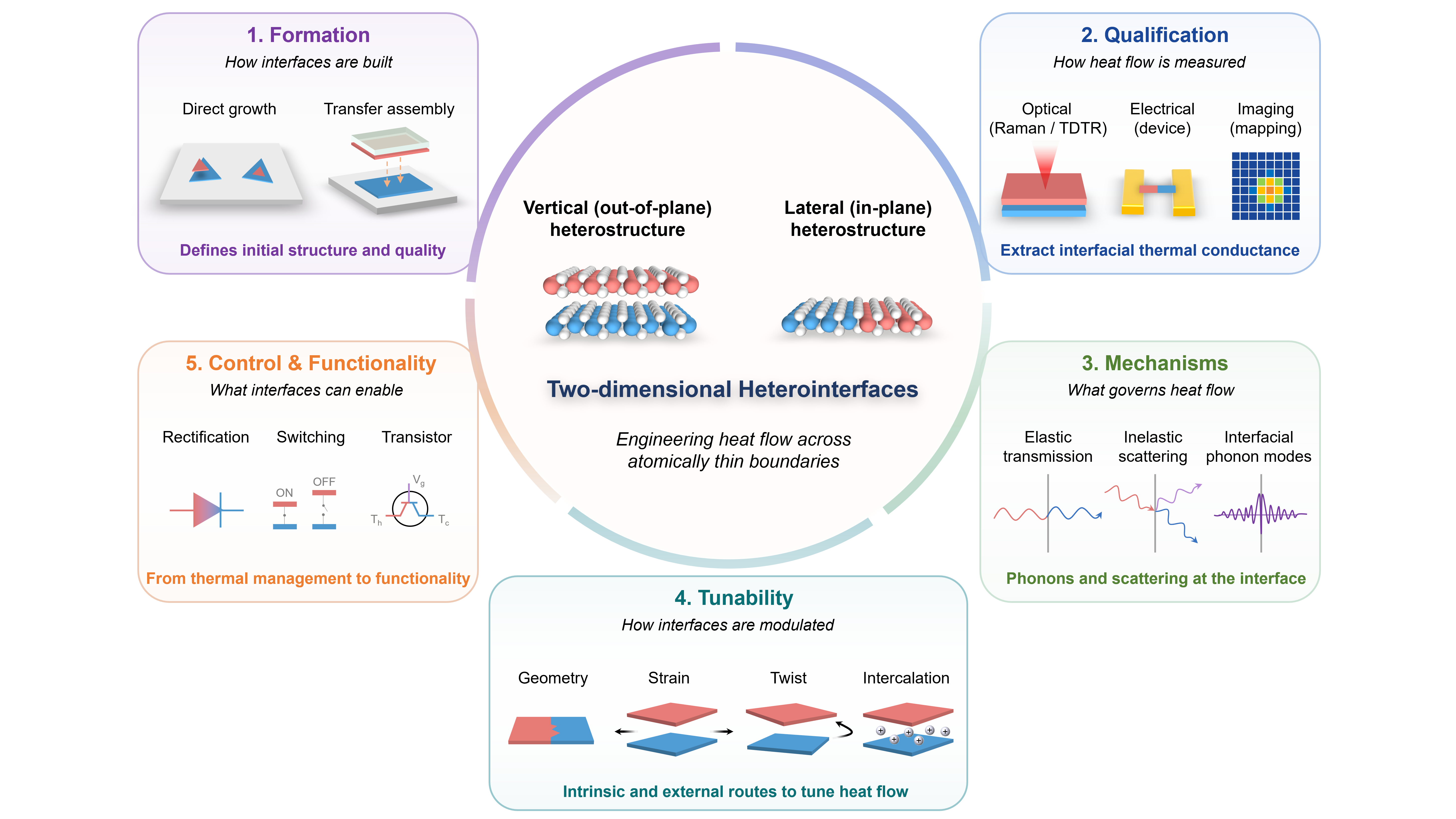
In this perspective, we examine interfacial thermal transport in 2D heterostructures through this design-oriented lens (Figure 1). We first discuss how direct growth and transfer assembly define the formation history of an interface and set the initial conditions for heat flow. We then consider the metrology required to quantify interfacial thermal transport, followed by the microscopic mechanisms that govern elastic transmission, inelastic scattering and interface-specific vibrational states. Finally, we discuss how intrinsic and external control of 2D heterointerfaces can be used to engineer heat flow and connect thermal dissipation to thermal functionality. We argue that the next stage of the field will be defined by a transition from measuring ITC as a passive material parameter to controlling it as an actively addressable degree of freedom.
Figure 1. Interfacial heat transport in 2D heterostructures as a designable degree of freedom. 2D heterointerfaces can be formed as vertically stacked van der Waals interfaces or laterally stitched in-plane junctions. Their thermal behavior is determined by a sequence of linked processes. Interface formation through direct growth or transfer assembly defines the initial structure and quality of the boundary. Thermal metrology, including optical, electrical and mapping-based approaches, enables interfacial heat transport to be quantified. Microscopic mechanisms such as elastic transmission, inelastic scattering and interface-specific phonon modes govern how vibrational energy crosses or is redistributed at the interface. These mechanisms can be modified through intrinsic and external tuning strategies, including interface geometry, strain, twist and intercalation. When such tunability is connected to device operation, 2D heterointerfaces can move beyond passive heat dissipation toward thermal functionality, including rectification, switching and transistor-like heat-flow control. 2D: two-dimensional; TDTR: time-domain thermoreflectance.
2. Interface Formation in 2D Heterostructures
2.1 Direct growth of 2D heterostructures
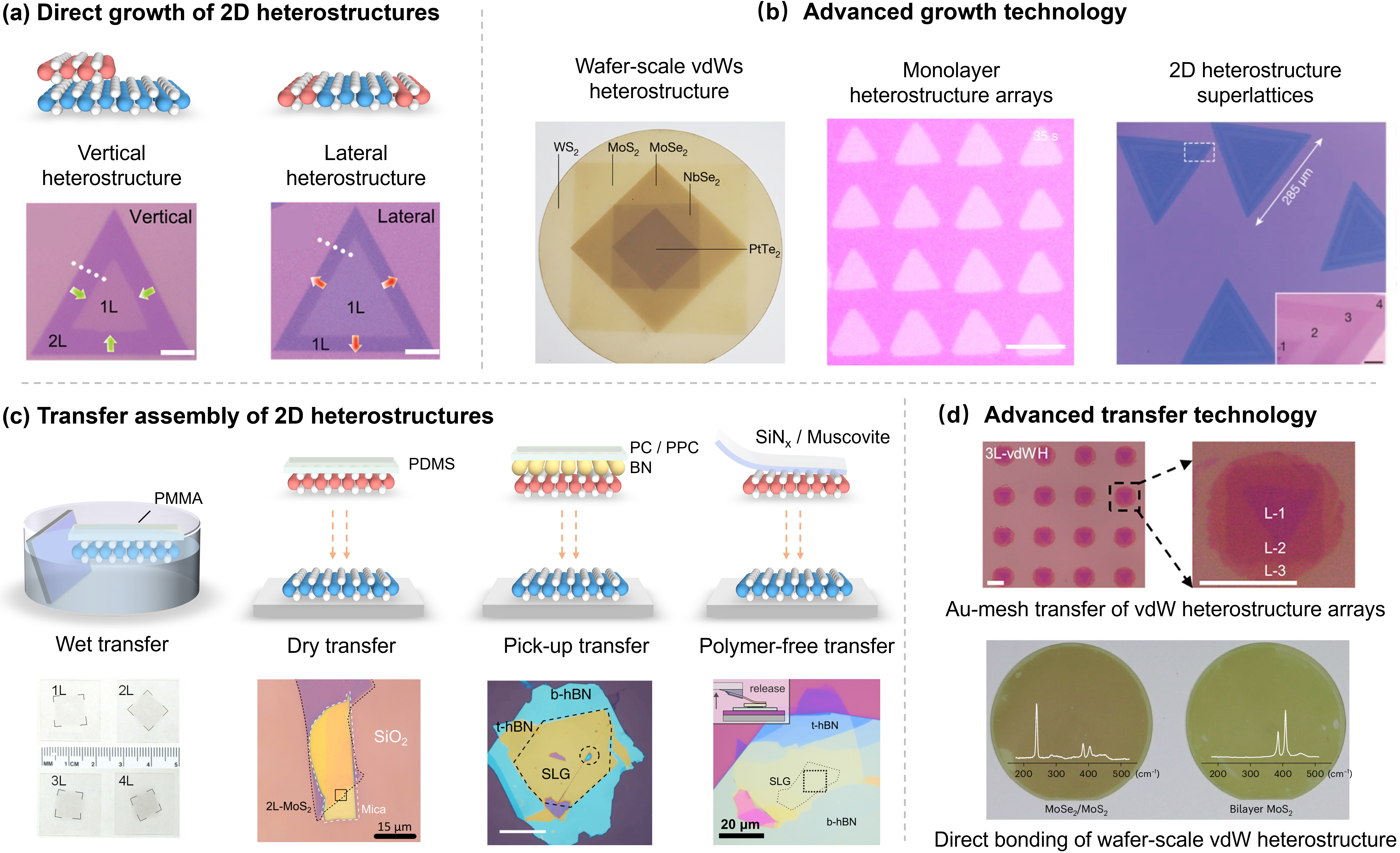
The direct synthesis of 2D heterostructures has evolved from serendipitous stacking into a sophisticated paradigm of material engineering, primarily driven by chemical vapor deposition and its advanced derivatives. The fundamental distinction between forming lateral (in-plane) versus vertical (out-of-plane) heterostructures is governed by the competition between growth kinetics and thermodynamics (Figure 2a), which together determine whether the second material forms a laterally stitched junction or a vertically stacked interface[27,36,37]. When active species diffuse to the edge of a pre-existing crystal, lateral epitaxy is favored, whereas nucleation on the basal plane promotes vertical stacking through vdW coupling[32,38-41]. Precursor ratio, supersaturation, and diffusion barriers can steer the nucleation pathway during growth, so lateral and vertical heterostructures are best understood as outcomes of a tunable kinetic-thermodynamic landscape rather than fixed consequences of material choice alone[26,42].

Figure 2. Formation routes and scalable assembly of 2D heterostructures. (a) Direct growth of 2D heterostructures. Representative optical images illustrate vertical and lateral growth outcomes. Reproduced with permission from reference[26]. Copyright © 2019 John Wiley and Sons; (b) Advanced growth technologies for deterministic and large-area 2D heterostructures. Direct synthesis has progressed from isolated heterostructure flakes toward wafer-scale vdW heterostructures, monolayer heterostructure arrays and patterned 2D heterostructure superlattices, providing a route toward scalable and spatially programmable integration. Reproduced with permission from reference[27]. Copyright © 2018 Springer Nature; reference[28]. Copyright © 2023 Springer Nature; reference[29]. Copyright © 2022 Springer Nature; (c) Transfer assembly of 2D heterostructures with wet transfer, dry transfer, pick-up transfer and polymer-free transfer approaches. Representative images show transferred monolayers and van der Waals stacks assembled through different transfer strategies. Reproduced with permission from reference[30]. Copyright © 2009 American Chemical Society; reference[31]. Copyright © 2014 IOP Publishing. Reproduced from reference[32,33]. CC BY 4.0; (d) Advanced transfer technologies for high-throughput and wafer-scale integration. Au-mesh-assisted transfer enables patterned vdW heterostructure arrays, whereas direct bonding and debonding strategies support wafer-scale assembly of 2D semiconductor heterostructures. Reproduced with permission from reference[34]. Copyright © 2021 American Chemical Society; reference[35]. Copyright © 2025 Springer Nature. 2D: two-dimensional; vdW: van der Waals; PC: polycarbonate; PPC: polypropylene carbonate; BN: boron nitride; SLG: single-layer graphene.
With this degree of synthetic control, direct growth is beginning to move well beyond the production of isolated heterostructure flakes and toward a broader regime defined by both scalable fabrication and structural programmability (Figure 2b). Wafer-scale heterostructure growth is now emerging as a realistic objective, pursued through routes such as metal-film precursor transformation[43-45], which offers a practical pathway to large-area conversion into layered heterostructures, and direct epitaxial growth[28,46], which seeks to extend crystallographic alignment and interfacial order across macroscopic dimensions. At the same time, direct synthesis is becoming increasingly capable of producing heterostructures with prescribed spatial organization. Substrate engineering, seeded nucleation, and defect- or laser-defined growth sites are making it possible to suppress random nucleation, align domains, and position junctions with growing determinism, thereby enabling ordered heterostructure arrays rather than isolated stochastic products[29,47]. In lateral systems, this trend reaches an even higher level of structural control in the form of superlattice growth, where periodic compositional modulation creates interface architectures that are both physically richer and synthetically more demanding than single junctions[27,41,48,49].
The importance of these developments extends well beyond fabrication itself. Large-area growth, ordered arrays, and superlattices collectively connect interface formation to reproducibility, statistical uniformity, and device-compatible placement, all of which become essential once 2D heterostructures are viewed not as individual model systems but as scalable materials platforms. They also open a distinct scientific opportunity. In particular, laterally modulated superlattices provide an exceptional platform for exploring coherent phonon transport and other wave-like heat-transfer phenomena that are difficult to access in isolated heterointerfaces, where structural periodicity and long-range order are limited. At the same time, these advances underscore how demanding direct synthesis remains. Deterministic placement, abrupt compositional transition, high crystallinity, defect suppression, and large-area uniformity must all be achieved simultaneously within a narrow synthesis window, making direct growth not only a route to scalable heterostructures but also one of the clearest demonstrations of how demanding true interface engineering has become.
2.2 Transfer assembly of 2D heterostructures
Transfer assembly provides the complementary route to interface formation and remains the most versatile strategy for integrating 2D heterostructures, because the constituent layers can be prepared separately and then combined with substantial freedom in material choice, stacking order, lateral placement, and relative orientation. In contrast to direct growth, where the interface is defined during crystallization under a shared growth window, transfer assembly creates the interface by bringing together pre-existing surfaces through deterministic stacking, and shifts the emphasis from growth compatibility to contact formation and alignment control.
Existing transfer routes are commonly grouped into wet transfer, dry transfer, pickup-assisted transfer and polymer-free transfer (Figure 2c). Wet-transfer methods, most commonly based on sacrificial polymer supports such as PMMA, established the basic workflow for relocating exfoliated or grown 2D crystals onto target substrates and for constructing early vdW stacks[30,50]. Their broad applicability made them foundational to the field, but also introduced persistent liabilities, including polymer residues, trapped adsorbates, wrinkles, and interfacial contamination[51]. Dry-transfer methods, typically implemented with viscoelastic stamps such as polydimethylsiloxane[31], polypropylene carbonate[52], or polycarbonate[32], reduced liquid exposure and markedly improved placement control, thereby becoming the basis of deterministic vdW assembly. Pickup-based approaches, especially h-BN-assisted pickup and hot-pickup strategies, advanced interface quality further by ensuring that buried internal interfaces are never directly exposed to sacrificial polymers or solvents[53,54]. More recently, low-contamination and polymer-free variants, including flexible SiNx-membrane and muscovite crystal platforms, have further expanded this toolbox by improving interface cleanliness while preserving the positional and rotational precision required for designed heterostructures[33,55]. These increasingly directional and contamination-minimized transfer routes have become particularly important for high-quality vdW heterostructures because they enable cleaner encapsulation, greater reproducibility, and precise twist-angle control, all of which are indispensable for twistronics and designer heterostacks.
Recent developments also make clear that transfer assembly is no longer confined to laboratory-scale manipulation of isolated flakes, but is beginning to evolve into a technologically meaningful route for large-area integration (Figure 2d). Dry exfoliation of large-area monolayers and heterostructure arrays has shown that transfer can be coupled to scalable preparation strategies capable of producing ordered 2D building blocks well beyond individual crystals[34,56,57]. At the same time, direct bonding and debonding of 2D semiconductors points to a more advanced paradigm in which epitaxially grown 2D semiconductor wafers can be bonded, released, and re-integrated without reliance on conventional adhesive-mediated transfer, thereby bringing 2D heterostructures closer to wafer-level processing and heterogeneous device integration[35]. These advances suggest that the future of transfer assembly will be defined not only by cleaner interfaces, but also by closer compatibility with semiconductor manufacturing. This shift is especially consequential because when transfer technologies become cleaner, more uniform, and more wafer-compatible, they cease to be merely convenient stacking tools and instead begin to function as enabling platforms for deliberately engineering ITC in integrated devices.
2.3 Interface formation as the starting point of thermal design
The thermal consequences of these formation routes arise from the interfacial structures they leave behind. In transfer-assembled vdW stacks, polymer residues, trapped adsorbates, wrinkles and local delamination can increase the effective interlayer spacing, reduce the real contact area and introduce spatially nonuniform coupling, thereby broadening or lowering the extracted ITC[58-62]. Cleaner pickup and polymer-free transfer can mitigate these effects by producing more intimate and reproducible layer-to-layer contact. In directly grown lateral heterostructures, the relevant structural variables are different. Edge disorder, dislocations, reconstructed motifs and alloyed transition regions define the width, bonding topology and chemical abruptness of the in-plane boundary, which can determine whether the interface behaves as a sharp phonon reflector, a diffuse transition layer or a selective vibrational filter[63-66].
These contrasting formation routes give rise to distinct scientific opportunities. Direct growth lays the foundation for scalable device integration and, by enabling sharp covalent interfaces, provides access to nanoscale phonon phenomena such as confinement, coherence, and tunnelling at chemically stitched boundaries. Transfer assembly, by contrast, opens an unprecedented opportunity to study phonon transport across vdW heterointerfaces because the interface itself can be deliberately reconfigured to produce new transport regimes and functionalities. From the perspective advanced in this article, neither route is intrinsically superior. Direct growth is likely to remain central to scalable integration and intrinsically sharp interface physics, whereas transfer assembly will remain the more powerful route for discovering and engineering tunable phonon transport in vdW systems. The future of the field will depend on using these two formation routes in complementary ways to transform 2D heterointerfaces from passive thermal boundaries into actively designable thermal elements.
3. Quantifying Interfacial Thermal Transport in 2D Heterostructures
Quantifying interfacial thermal transport in 2D heterostructures is challenging because the heat-carrying interface is atomically thin, weakly accessible and embedded within a complex multilayer environment. The thermal signal from a single heterointerface is often small, while the measured response inevitably contains contributions from the adjoining 2D layers, metal contacts, encapsulation layers and supporting substrates. In vertical stacks, the interface of interest is frequently buried beneath the surface, while in lateral heterostructures, heat must be driven and detected across a nanoscale in-plane boundary. As a result, reliable quantification requires both sensitive thermometry and careful control of optical absorption, heat-flow geometry, background thermal resistances and model parameter coupling.
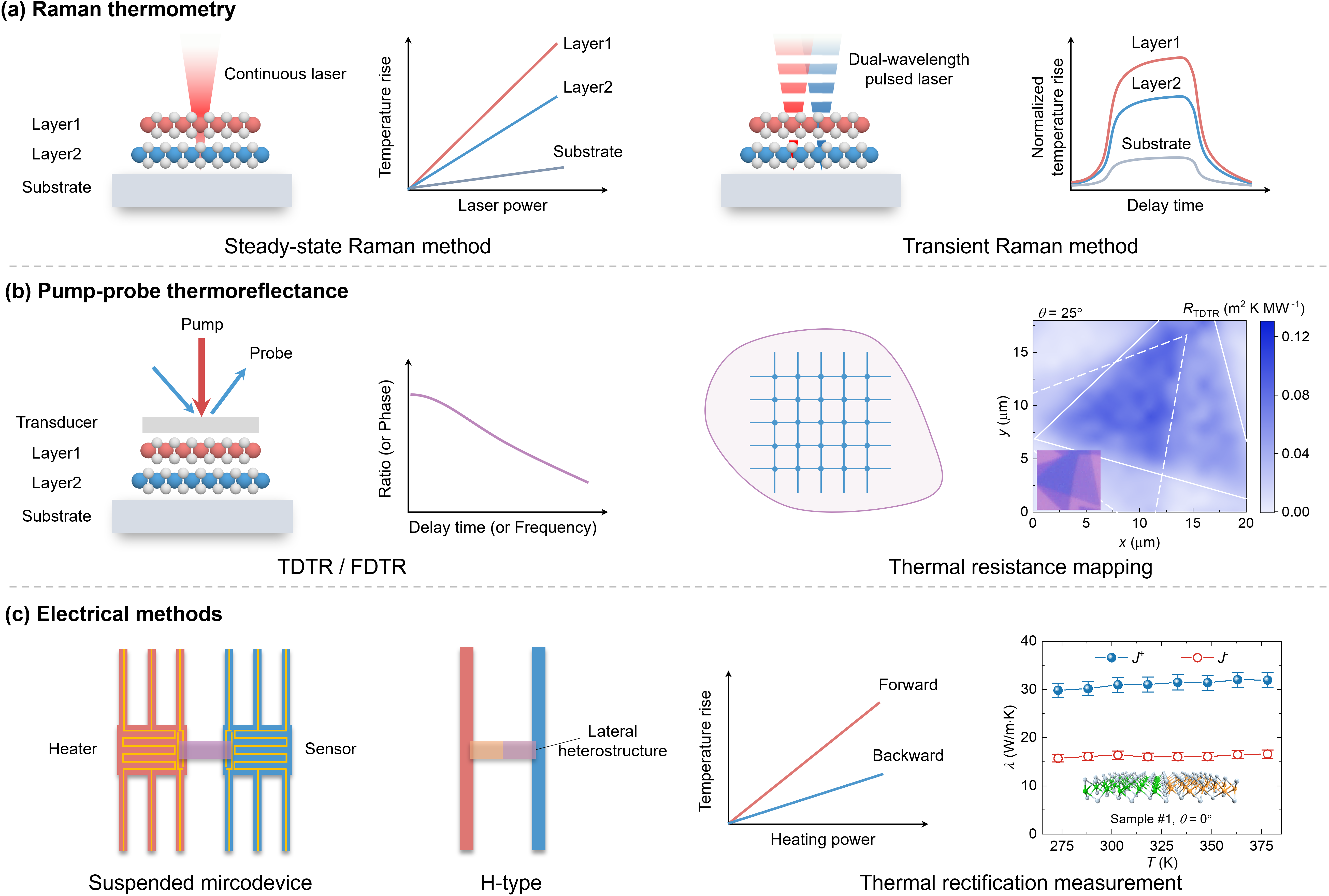
3.1 Raman thermometry
Raman thermometry has been one of the most widely used approaches for 2D materials since the landmark optothermal Raman measurements on monolayer graphene established the method as a noncontact route to thermal characterization[67-69]. Its basic principle is to infer temperature from Raman peak shifts while laser heating drives the thermal response (Figure 3a). A particular advantage in 2D heterostructures is the fingerprint nature of Raman spectroscopy, which often allows the temperature rise of different constituent layers to be measured separately within the same vdW stack[70]. This layer selectivity makes it possible to directly determine the temperature difference between adjacent layers and thereby access interfacial thermal transport with a level of physical specificity that is difficult to achieve in many other optical methods[58,71-74]. This capability has also been extended to electrically driven heterostructures, where integrated Joule heating combined with layer-resolved Raman thermometry enables the thermal resistance between individual 2D monolayers in a vdW stack to be identified directly[70,75,76].

Figure 3. Experimental approaches for quantifying interfacial thermal transport in 2D heterostructures. (a) Raman thermometry methods. In steady-state Raman thermometry, a continuous laser simultaneously heats and probes the heterostructure, and the temperature rise of different layers or the substrate is extracted from Raman peak shifts as a function of laser power. In transient Raman thermometry, pulsed or dual-wavelength excitation tracks the time-dependent thermal response, reducing reliance on laser absorption coefficient; (b) Pump-probe thermoreflectance methods. In TDTR and FDTR measurements, a pump beam periodically heats a metal transducer deposited on the heterostructure, while a delayed probe beam monitors the transient reflectance response. Fitting the delay- or frequency-dependent signal with a multilayer heat-transfer model enables extraction of interfacial thermal resistance. Spatial scanning further allows thermal resistance mapping across large-area 2D heterostructures. Reproduced with permission from reference[13]. Copyright © 2026 National Academy of Sciences; (c) Electrical thermal metrology. Suspended microdevice platforms measure heat flow through a sample bridging calibrated heater and sensor membranes, enabling high-accuracy thermal conductance measurements. H-type devices provide a simpler geometry for probing directional heat flow across lateral heterostructures and can be used to quantify forward and backward thermal transport, including thermal rectification. Reproduced with permission from reference[24]. Copyright © 2022 National Academy of Sciences. 2D: two-dimensional; TDTR: time-domain thermoreflectance; FDTR: frequency-domain thermoreflectance.
The main limitation is that the absorbed laser power is often difficult to determine accurately, especially in supported multilayer stacks, which directly limits quantitative accuracy[77-79]. This challenge has motivated the development of transient optothermal Raman, including state-differential Raman[80,81], flash Raman[82,83] and dual-wavelength flash Raman[84,85] schemes, which reduce dependence on absolute absorption and improve sensitivity to interfacial transport (Figure 3a). Even so, Raman methods remain intrinsically better suited to situations in which heat diffuses away from the laser-heated region in a relatively symmetric manner, and are much less straightforward for quantifying heat conduction across lateral heterointerfaces. Under such conditions, dual-wavelength Raman approaches that enable spatial mapping of the in-plane temperature field during laser heating may provide a viable pathway toward overcoming this limitation[86].
3.2 Pump-probe thermoreflectance
Time-domain thermoreflectance (TDTR) and frequency-domain thermoreflectance (FDTR) have become standard tools for quantifying heat transfer in thin films and interfaces[87,88]. Their basic principle is to use modulated optical heating and reflectance-based thermometry to probe transient or frequency-dependent thermal response (Figure 3b), which is then interpreted through a multilayer heat-transfer model[89-91]. For 2D heterostructures, these methods are particularly well suited to supported vertical stacks, where the thermally relevant interface is buried beneath the surface and the dominant process of interest is cross-plane heat flow rather than lateral diffusion.
A major strength of pump-probe thermoreflectance is its combination of interface sensitivity and experimental throughput[92-97]. Because the technique directly tracks the thermal response of the multilayer stack without requiring full spectral acquisition at every position, it is well suited to rapid spatial mapping over extended sample areas, which is especially valuable for 2D heterostructures whose interface quality and thermal coupling are often spatially nonuniform[95,98]. This capability has recently enabled mapping-based studies of twisted vdW heterointerfaces (Figure 3b), including the observation of anomalously enhanced ITC in MoS2/WS2 heterobilayers[13]. These strengths are balanced by well-known limitations. Interpretation is strongly model dependent, parameter covariance in multilayer fitting can be substantial, and conventional implementations usually require a metal transducer layer that may perturb the native interface[90]. In addition, the measured signal represents a finite subsurface sampling volume rather than an atomically localized interface, which can become a significant issue in strongly heterogeneous systems[99]. For this reason, recent transducerless, wideband, and beam-offset variants are especially relevant to 2D materials[100-103], where buried-interface sensitivity, spatial mapping, and reduced measurement perturbation are all important.
3.3 Electrical methods
Electrical thermal metrology remains one of the most accurate routes for quantifying heat transport in suspended low-dimensional systems. In its classical form, the suspended microdevice or suspended micro-bridge approach measures heat flow between two thermally isolated membranes bridged by the sample (Figure 3c), thereby defining a relatively well-controlled thermal circuit and enabling high-precision extraction of thermal conductance or thermal conductivity[104,105]. This framework has been central to the measurement of low-dimensional materials because it minimizes parasitic substrate leakage and directly links the applied heating power to the resulting temperature response through calibrated electrical sensing[106-109].
For 2D heterostructures, the importance of electrical methods extends beyond accuracy. Unlike optical approaches, which are naturally best matched to laser-driven diffusion around a local heating spot, electrical methods are inherently compatible with directional heat-flow geometries. This makes them particularly valuable for lateral heterostructures, where the central question is often how efficiently heat is transmitted across an in-plane interface. In this sense, electrical metrology helps fill a critical gap left by optical methods by providing a more direct route to quantifying cross-interface heat conduction in laterally stitched junctions. This capability has become especially important in studies of thermal rectification and electrically driven reversible phonon transport, where heat must be driven and sensed along two opposite directions through the same heterointerface[110-112].
Within this family, H-type device configurations are especially useful in this regard because they establish a device-oriented fabrication paradigm in which sensor structures can be integrated directly with the heterostructure, making the method practical for small or fragile interfaces that are difficult to study in conventional suspended-membrane architectures (Figure 3c)[17,24,113-116]. This is particularly valuable for lateral heterojunctions and other integrated 2D devices, where the thermally relevant interface may be too small or too difficult to manipulate reliably within a conventional suspended-membrane architecture[24,113]. The principal limitations of electrical methods remain fabrication complexity, thermal contact resistance between the sample and electrodes, and parasitic heat loss through radiation, metal leads, or residual substrate coupling. However, for many 2D heterostructures, these limitations are offset by the fact that electrical platforms provide one of the most direct ways to probe directional phonon transport across a specific interface under device-relevant conditions.
Table 1 summarizes the main experimental approaches for quantifying interfacial thermal transport in 2D heterostructures. These methods differ in their suitable interface geometry, extracted thermal quantity, probing scale, and dominant sources of uncertainty. The comparison highlights that ITC is usually inferred from a broader thermal response rather than measured as an isolated interface property, making method selection and uncertainty analysis central to reliable quantification.
Table 1. Comparison of experimental methods for quantifying interfacial thermal transport in 2D heterostructures.
| Method | Suitable geometry | Main extracted quantity | Probing scale | Main uncertainties |
| Steady-state Raman method | Suspended/supported vertical heterostructures | Thermal conductivity, ITC | Optical spot size, usually sub-µm to µm | Laser absorption, Raman temperature calibration and laser spot profile |
| Transient Raman method | Thermal diffusivity, ITC | Weak transient Raman signal and laser spot profile | ||
| TDTR/FDTR | Supported vertical heterostructures | In-plane/cross-plane thermal conductivity, ITC | Pump/probe spot and thermal penetration depth, typically µm lateral scale and tens of nm to µm depth scale | Model dependence parameter covariance, transducer thickness and thermal properties |
| Suspended microdevice method | Suspended lateral heterostructures | Directional thermal conductance, Thermal rectification ratio | Device-defined in-plane path, typically µm scale | Fabrication complexity, thermal contact resistance and radiative heat loss |
| H-type method | Fabrication complexity, thermal contact resistance and parasitic heat leakage through metal leads |
2D: two-dimensional; ITC: interfacial thermal conductance; TDTR: time-domain thermoreflectance; FDTR: frequency-domain thermoreflectance.
3.4 Outlook for future metrology
The most consequential advances in this area are likely to come from metrologies that are simultaneously spatially resolved, high-resolution, time-resolved, and operando. In practice, spatial mapping and spatial resolution are closely linked. Many of the most interesting structural motifs in 2D heterostructures, including moiré superlattices[117], reconstructed boundaries[118], one-dimensional (1D) channels[119], and nanoscale hot spots in operating devices[120], fall below the spatial scale of conventional optical thermal probes. This motivates the convergence of thermal metrology with near-field and scanning-probe methods, such as tip-enhanced Raman methods[117,121] and optical pump-probe-inspired atomic force microscopy schemes[122]. A related opportunity lies in coupling electrical and optical methods. Electrical techniques remain well suited to driving directional heat flow across lateral heterointerfaces, whereas optical readout is better suited to imaging the resulting temperature field[123]. Higher spatial resolution will also be increasingly important for measuring local junction temperatures in 2D devices, where nanoscale thermal nonuniformity may strongly influence switching, reliability, and functional stability.
Time resolution is likely to become equally important. If tunable interfacial conductance is to support thermal switches, thermal transistors, or dynamically reconfigurable heat management, then metrology must move beyond static or quasi-static characterization toward opto-electrical hybrid measurements, in which electrical driving and optical or local thermal readout are combined to resolve how interfacial heat flow evolves in real time. The objective is to capture how that parameter changes under gate bias, current flow, optical excitation, structural relaxation, or other external fields[25,124]. In this broader sense, the future of thermal metrology will depend on bridging large-area mapping, nanoscale spatial resolution, and real-time operando measurement within a single experimental framework.
4. Mechanisms of Heat Flow Across Atomically Thin Heterointerfaces
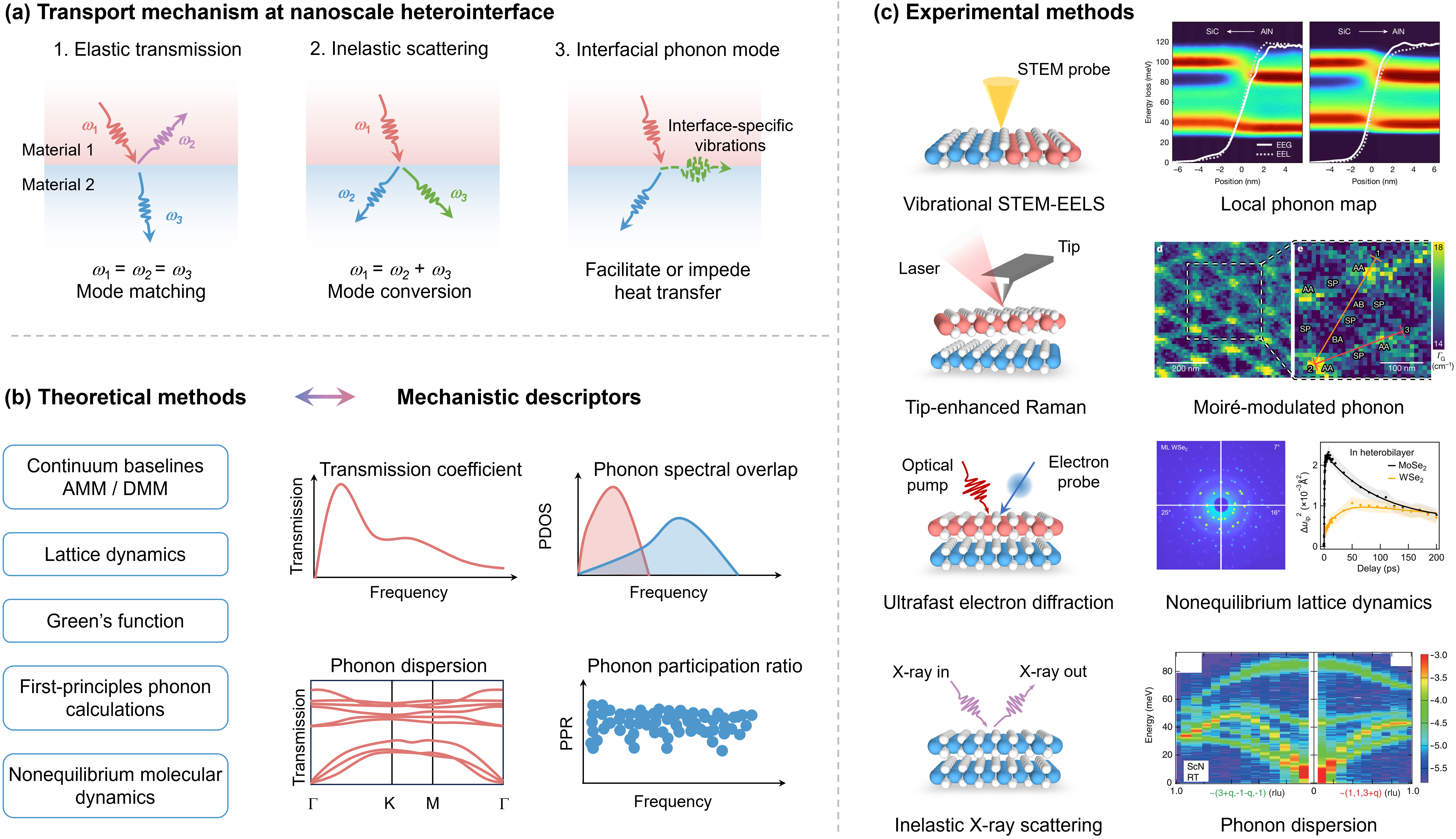
Interfacial heat transport at the nanoscale differs fundamentally from that across conventional bulk interfaces[11,125,126]. At atomically thin heterointerfaces, heat flow depends not only on the bulk properties of the adjoining materials, but also on the microscopic structure of the interface itself, including bonding topology, local registry, and spatial heterogeneity. This is especially true for 2D heterostructures, where weak vdW coupling, moiré reconstruction, interfacial corrugation, and low-dimensional confinement all amplify the role of local interfacial physics. Atomically thin heterointerfaces also often lie outside the assumptions of simple diffuse or continuum heat flow. At nanoscale interfaces, the boundary can selectively transmit, reflect, convert, or localize vibrational energy. Interfacial heat transport becomes highly sensitive to vibrational spectral overlap, bond stiffness contrast, interfacial force constants, and interface-specific phonon modes (Figure 4a).

Figure 4. Mechanistic understanding of heat flow across nanoscale heterointerfaces. (a) Transport mechanisms at nanoscale heterointerfaces. Elastic transmission occurs when an incident phonon transmits across the interface without changing frequency, provided that vibrational modes on the two sides are sufficiently matched. Inelastic scattering allows energy transfer through mode conversion, in which an incident phonon couples to multiple modes with different frequencies. Interface-specific phonon modes can further localize vibrational energy at the boundary and either facilitate or impede interfacial heat transfer; (b) Theoretical methods for analyzing interfacial heat transport mechanisms. Continuum models, lattice dynamics, Green’s-function approaches, first-principles phonon calculations and nonequilibrium molecular dynamics provide complementary descriptions of interfacial phonon transport. Their outputs include transmission coefficients, phonon spectral overlap, phonon dispersion and phonon participation ratios, which help identify whether heat flow is governed by harmonic matching, inelastic scattering, localized vibrational modes or structural disorder; (c) Experimental methods for probing interfacial phonon dynamics. Vibrational STEM-EELS provides nanoscale phonon mapping near interfaces, tip-enhanced Raman spectroscopy resolves moiré-modulated and localized vibrational modes, ultrafast electron diffraction tracks nonequilibrium lattice dynamics, and inelastic X-ray scattering measures phonon dispersion and collective excitations. Reproduced from reference[127,128]. CC BY 4.0. Reproduced with permission from reference[117]. Copyright © 2021 Springer Nature; reference[129]. Copyright © 2018 American Physical Society. STEM: scanning transmission electron microscopy; EELS: electron energy loss spectroscopy; AMM: acoustic mismatch model; DMM: diffuse mismatch model.
4.1 Core transport mechanisms at nanoscale heterointerfaces
The most basic starting point for understanding interfacial heat transport is elastic vibrational transmission[130,131]. In this picture, phonons transfer energy across the interface when modes on the two sides are compatible in frequency, polarization, and velocity. Elastic transmission is most effective when the adjoining materials have overlapping low-frequency phonon spectra, comparable acoustic impedances, and an ordered interface that preserves efficient coupling between incident, reflected, and transmitted modes. This framework captures the importance of vibrational matching and helps explain why interfaces with better low-frequency overlap often exhibit higher thermal conductance[132,133]. For 2D heterostructures, it is especially relevant to long-wavelength acoustic modes and to out-of-plane vibrations that couple directly across vertically stacked layers[9,13,94].
Elastic transmission, however, is rarely sufficient on its own. When the two materials are strongly mismatched in their vibrational spectra, local anharmonicity is large, or interface disorder relaxes momentum selection, inelastic phonon scattering becomes increasingly important[134-138]. Rather than requiring one-to-one mode matching, inelastic processes redistribute thermal energy among different phonon branches during transmission and can open channels inaccessible within a purely harmonic picture. Such processes can substantially enhance heat transfer across mismatched interfaces, especially in atomically thin systems where broken symmetry, local reconstruction and interface-specific perturbations strengthen mode conversion[13,15].
A further level of complexity arises from interfacial phonon modes and localized interface vibrations[139-143]. These excitations are generated or strongly reshaped by the interface itself rather than simply inherited from either adjoining material. Their influence on heat flow depends on whether they act as bridge states or trapping states. Modes that overlap spectrally and spatially with phonons on both sides of the interface can mediate mode conversion and facilitate interfacial energy transfer, whereas highly localized modes that couple strongly to only one side tend to trap vibrational energy and enhance reflection or diffuse scattering. At the nanoscale, the interface is not merely a filter for bulk phonons, but can also host vibrational states with their own thermal role.
These general mechanisms take different forms in vertical and lateral 2D heterointerfaces. For vertical heterointerfaces, the central issue is cross-plane energy transfer across a weakly bonded interlayer gap. Because adjacent layers are linked primarily through vdW interactions, transport depends strongly on interfacial force constants, local spacing, and the extent of real contact[61,144]. Twist and lattice mismatch further modulate local atomic registry and generate moiré reconstruction, so that heat flow is governed by a spatially varying landscape of interfacial coupling and nonequilibrium mode populations[117].
Lateral heterointerfaces are governed by a different physical setting. Here heat does not cross a weakly bonded gap, but propagates through a chemically stitched or reconstructed transition region within the plane. The decisive factors become the width and atomic structure of that boundary, including mass contrast, bond-stiffness variation, alloying, defects, and 1D interface motifs[66,145,146]. Depending on how the junction is formed, the interface may behave as a sharp phonon reflector, a distributed transition layer, or a selective vibrational filter[24].
4.2 Theoretical methods for analyzing interfacial heat transport mechanisms
Mechanistic understanding has relied on a combination of theoretical and atomistic tools. At the most approximate level, acoustic and diffuse mismatch models remain useful as baseline descriptions of interfacial transmission[130,131]. Their value lies mainly in the physical intuition they provide, but for atomically thin heterointerfaces, where local registry, weak bonding, reconstruction, and interface-specific vibrational states all become important, such continuum-level treatments are rarely sufficient on their own.
More detailed insight typically comes from lattice dynamics[147,148], Green’s function approaches[149,150], first-principles phonon calculations[151,152], and nonequilibrium molecular dynamics[153-155]. These methods resolve phonon transmission spectra, spectral heat flux, local density of states, interfacial force constants, mode-resolved contributions, and the role of anharmonicity (Figure 4b). In doing so, they shift the question from the extraction of a single conductance value to a more revealing set of issues, namely which modes carry heat, where scattering occurs, and how specific structural features modify the available transport pathways.
For 2D heterostructures, descriptors such as spectral overlap factors[132,156], phonon participation ratios[157,158], and mode-resolved transmission coefficients[135,159] have become especially useful for distinguishing whether an observed trend originates primarily from harmonic matching, stronger interlayer coupling, enhanced inelastic scattering, or interface-specific vibrational states (Figure 4b). These descriptors should be interpreted together because a single trend in ITC may reflect several coupled mechanisms. Spectral overlap, for example, captures the availability of vibrational states for elastic exchange, but it does not determine transmission unless interfacial coupling, polarization, group velocity, and real contact quality are also considered.
4.3 Experimental methods for analyzing interfacial heat-transport mechanisms
Experimental access to interfacial heat-transport mechanisms remains challenging because the relevant phonons are often highly localized in space, evolve on ultrafast timescales, and are embedded in structurally complex interfaces (Figure 4c). Among the emerging approaches, vibrational scanning transmission electron microscopy (STEM)-electron energy loss spectroscopy (EELS) has become especially promising[160,161]. By combining electron microscopy with vibrational spectroscopy, it can access phonon-related excitations with nanometer and, in favorable cases, sub-nanometer spatial resolution, making it unusually well suited to reconstructed interfaces, defect-rich boundaries, and other localized motifs central to nanoscale heat transport[142,162-164]. Recent studies have gone beyond static vibrational imaging to probe phonon transport dynamics across interfaces directly, indicating that electron microscopy can begin to resolve where temperature drops and inelastic scattering are concentrated at nanometer scales[127].
A broader experimental landscape is also beginning to take shape. Ultrafast electron diffraction and diffuse-scattering methods provide femtosecond access to nonequilibrium lattice dynamics and have been used to follow interlayer energy flow and coherent acoustic phonon evolution in layered systems[128,165,166]. Tip-enhanced Raman spectroscopy has shown that moiré-modulated lattice dynamics can be visualized below the diffraction limit, as demonstrated by nano-Raman imaging of localized phonon behavior in low-angle twisted bilayer graphene[117]. Momentum-resolved probes, including inelastic X-ray scattering and resonant inelastic X-ray scattering, provide a complementary perspective by resolving phonon dispersion and other lattice excitations in reciprocal space[129,167-169]. Although these methods are not yet routine thermal metrologies in the conventional sense, they increasingly allow the field to probe the phonons themselves rather than infer their role only through effective thermal parameters.
4.4 Outlook for mechanistic studies of interfacial heat transport
Mechanistic studies are likely to move first from idealized interfaces toward formed interfaces, meaning models and measurements that explicitly incorporate growth history or transfer history. A parallel shift will be from average descriptors toward interface-specific excitations. The field is moving from asking only how much heat crosses an interface to asking which phonons carry that heat, how they are transformed, and where their transport is spatially concentrated. Methodologically, predictive understanding will require multiscale theoretical frameworks that preserve atomistic realism while remaining tractable on experimentally relevant length and time scales. This is where machine-learning interatomic potentials are becoming especially important[170,171]. Conventional empirical potentials are often too rigid to capture weak interlayer coupling, registry dependence, and strongly structure-sensitive interface dynamics with sufficient fidelity, whereas first-principles methods remain too computationally expensive for realistic nonequilibrium simulations. Machine-learning interatomic potentials provide a route between these limits by retaining near-first-principles accuracy while extending simulations to much larger systems and richer structural landscapes. More broadly, the future of this area will depend on tighter integration between theory and experiment, so that interface phonons and nonequilibrium lattice dynamics can be observed directly and interpreted in structurally realistic models. The longer-term opportunity is to establish a predictive framework in which interfacial heat transport can be designed through control of bonding topology, local registry, morphology, and external perturbation.
5. Engineering Interfacial Heat Flow for Device Functionality in 2D Heterostructures
If interfacial heat transport in 2D heterostructures is governed by local bonding, interfacial morphology, and vibrational coupling, then the natural next question is how those quantities can be deliberately controlled. For vdW heterostructures, this question is especially compelling because the interface remains structurally accessible even after the constituent layers have been assembled. In this sense, interface engineering can become the attempt to identify which features of the interface are written into it during formation, which can be modified afterward, and how these control approaches can be used to shape heat flow in a reproducible and functionally meaningful way.
5.1 Engineering interfacial heat flow through intrinsic and external control
For vertical heterointerfaces, a useful starting point is to distinguish between intrinsic structural and chemical tuning and external, potentially reversible tuning. The first class includes factors such as local registry, defects, doping, and interfacial chemistry (Figure 5a). These variables define the interfacial state at a more fundamental level because they are embedded in the composition or local bonding environment of the junction itself. Local registry determines how atomic motion is coupled across the interface at the smallest scale[61,144]. Defects and dopants can alter vibrational spectra, broaden available scattering channels, or change local force constants[172-175]. Interfacial chemistry and functionalization may further shift selected regions of a junction away from the purely vdW limit and toward mixed bonding environments with stronger local coupling[176,177]. Such factors are often introduced during growth, assembly, or post-processing, and are better viewed as parameters written into the interface than as variables that can be continuously tuned afterward[178-180].
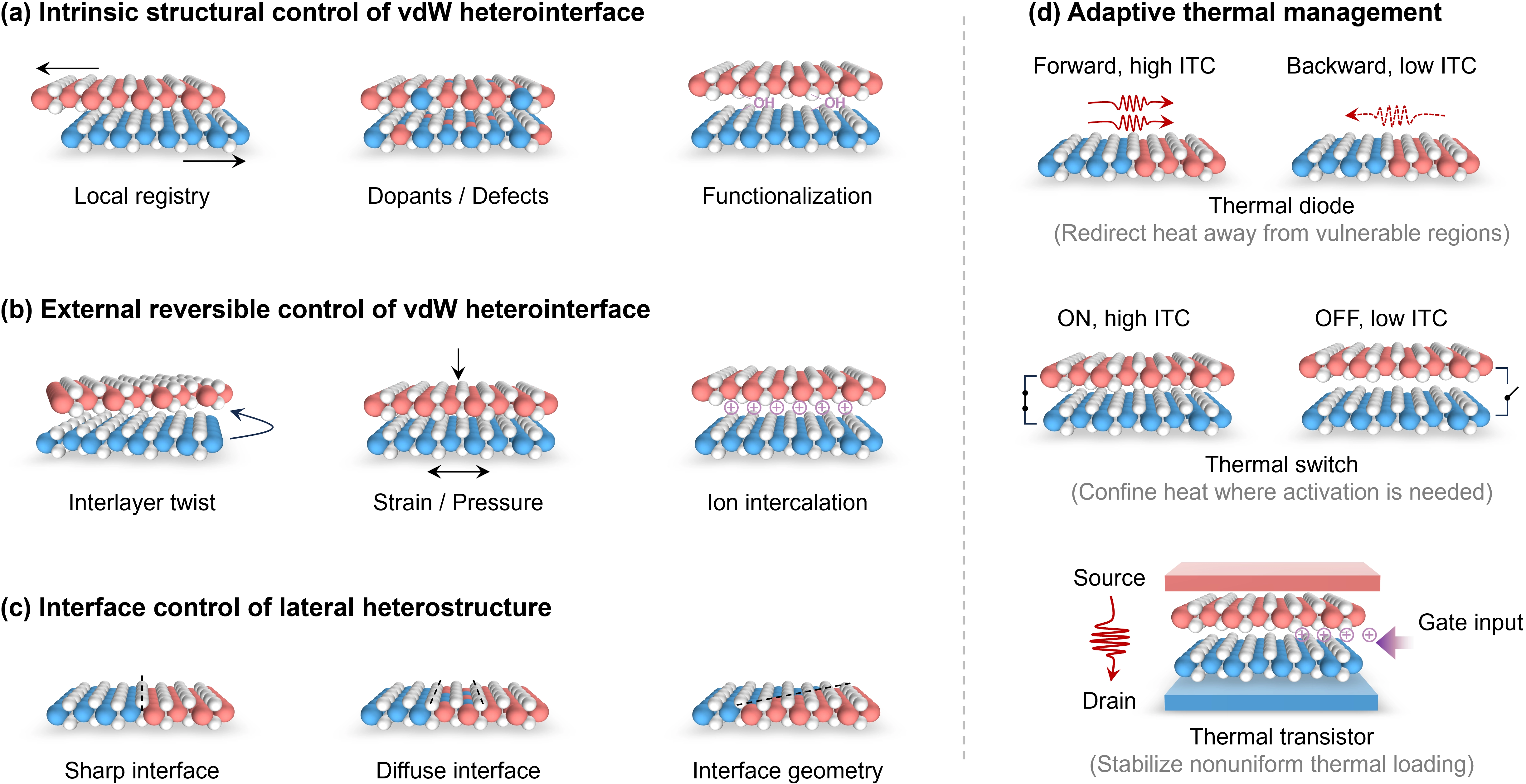
Figure 5. Engineering interfacial heat flow toward adaptive thermal functionality in 2D heterostructures. (a) Intrinsic structural control of vertical vdW heterointerfaces. Local registry, dopants or defects, and interfacial functionalization modify the local bonding environment, vibrational coupling and phonon-scattering landscape across the interface, thereby defining thermal transport properties that are largely written into the junction during growth, assembly or post-processing; (b) External and reversible control of vdW heterointerfaces. Interlayer twist, strain or pressure, and ion intercalation provide routes to reconfigure interfacial spacing, contact, charge environment and phonon coupling after the heterostructure has been formed. These perturbations can potentially enable dynamic modulation of ITC; (c) Interface control in lateral heterostructures. In-plane heterointerfaces can be engineered through the abruptness of the elemental transition, the width of a diffuse interface and the geometry of the boundary. Because heat must propagate across a chemically stitched and often asymmetric in-plane junction, lateral heterostructures provide a natural platform for direction-dependent heat flow and thermal rectification; (d) Adaptive thermal-management concepts enabled by tunable heterointerfaces. A thermal diode allows forward heat flow with high ITC while suppressing backward transport. A thermal switch reversibly toggles between high- and low-conductance states to confine or release heat as needed. A thermal transistor uses an external gate input to modulate heat current between source and drain, providing a route toward active control of nonuniform thermal loading. 2D: two-dimensional; vdW: van der Waals; ITC: interfacial thermal conductance.
A second class of control is more distinctive to vdW heterostructures because it acts on the interface from the outside and can be made reversible (Figure 5b). Twist is the clearest example[95,181,182]. By changing relative rotational alignment without changing composition, twist reshapes local stacking registry, transforms a nominally uniform interface into a laterally modulated coupling landscape, and reconfigures the phonon scattering channels[13,94,96,183]. Strain provides a similarly powerful route by altering phonon dispersion, interlayer spacing, and local contact pressure[184,185]. Ion intercalation offers another potentially powerful means of control by modifying interlayer separation, charge environment, and vibrational coupling through species inserted between adjacent layers[186-190]. Its ability to strongly modulate interfacial thermal transport has so far been explored mainly in homogeneous or symmetric layered systems, whereas its extension to heterostructures remains largely open. The broader significance of these external routes is that they preserve the idea of the interface as a thermally active element rather than a static boundary.
The control problem is different for lateral covalent heterointerfaces. In this case, the interface is not a weakly bonded gap between stacked layers, but a chemically stitched in-plane boundary through which heat must propagate. The most consequential design variables are the abruptness of elemental transition, the width and structure of the interfacial region, and the angle between the boundary and the imposed heat-flow direction (Figure 5c)[24,32,38,40,41,191,192]. A sharp interface, a diffuse alloyed transition, and a boundary containing extended defects or reconstructed motifs will not present the same phonon landscape to an incoming heat current[9,66,193-195]. Their significance is further enhanced by the fact that lateral 2D heterointerfaces often possess an intrinsic structural asymmetry along the heat-flow direction. This makes them especially attractive for thermal rectification, because forward and reverse heat flow can experience different phonon scattering landscapes across the same boundary[24,110,196-198]. This asymmetry is often more directly expressed than in vertically stacked vdW interfaces, because heat in a lateral junction must traverse an in-plane boundary whose composition and bonding can differ along the forward and reverse directions. In this sense, lateral heterostructures provide a particularly promising platform for realizing direction-sensitive thermal functions in atomically thin systems.
Representative values further illustrate the broad range of interfacial heat-transport magnitudes and modulation responses in 2D heterointerfaces (Table 2). For vertical vdW interfaces, reported ITC values range from only a few MW m-2 K-1 in weakly coupled or highly mismatched stacks to several tens of MW m-2 K-1 when contact quality, encapsulation, or interfacial coupling is improved. External perturbations such as twist, strain, and intercalation can further modify the effective conductance by changing spectral overlap, interlayer spacing, and disorder. For lateral covalent interfaces, directly measured ITC values remain less common, and many studies instead report effective in-plane thermal conductance, thermal conductivity variation, or thermal rectification. Even so, these results show that boundary abruptness, defect structure, composition profile, and interface geometry can strongly influence phonon transmission across chemically stitched junctions. The values summarized in Table 2 are merely intended as representative benchmarks, and direct comparison should take into account differences in interface geometry, measurement protocol, and reported thermal quantity.
Table 2. Representative interfacial thermal transport values and modulation effects in 2D heterointerfaces.
| Interface type | Representative system and control route | ITC value or modulation magnitude | Measurement or simulation method | Control mechanism | Ref. |
| vdW interface | Gr/MoS2 heterobilayer | 11 ± 3 MW m-2 K-1 | Steady-state Raman | / | [70] |
| Gr/WSe2 heterobilayer | 5 ± 3 MW m-2 K-1 | ||||
| MoS2/WSe2 heterobilayer | 9 ± 3 MW m-2 K-1 | ||||
| Monolayer WS2/multilayer h-BN | 7 MW m-2 K-1 | TDTR | [91] | ||
| Monolayer WSe2/multilayer h-BN | |||||
| Multilayer Gr/h-BN | 98.0 ± 7.6 MW m-2 K-1 | NEMD | [144] | ||
| Monolayer MoS2/multilayer h-BN | 74 ± 25 MW m-2 K-1 | Steady-state Raman | [72] | ||
| Local registry in multilayer Gr/h-BN | Registry dependent ITC with ABp > DW > AB > AA | NEMD | Change interlayer force constants and mode coupling | [144] | |
| Defective Gr/MoS2 heterobilayer | Increase ITC by 80% with 5% concentration of C-vacancy defect | AEMD | Reshape phonon spectral overlap | [173] | |
| Multilayer Gr/h-BN with atom diffusion | Composition diffusion can improve ITC by up to ~70% | NEMD | Modify phonon spectral overlap | [176] | |
| Functionalized Gr/h-BN heterointerface | NH2 functionalization enhances ITC by over 800% | NEMD | Strengthen vdW coupling | [177] | |
| Twisted MoS2/WS2 heterobilayer | Interlayer twist enables a 2.5-fold increase in ITC | TDTR | Activates efficient phonon conversion through inelastic scattering | [13] | |
| Strained graphene Kirigami heterostructure | ITC can be continuously regulated by in-plane tensile strain | AEMD | Change interfacial interaction density and delocalized phonon-mode distribution | [184] | |
| MoS2/organic interface | ITC is one order of magnitude lower than MoS2 single crystal | Laser Flash Method | Induce structural disorder and increased phonon scattering rate | [190] | |
| Covalent interface | Gr/h-BN monolayer | 4.3 GW m-2 K-1 | NEMD | / | [198] |
| Gr/BCN monolayer | 4.9 GW m-2 K-1 | ||||
| Gr/BC2N monolayer | 4.0 GW m-2 K-1 | ||||
| Gr/h-BN monolayer with interface diffusion | Interface diffusion reduces TC of heterostructure | NEMD | Anderson localization of phonons | [66] | |
| Periodic MoS2/MoSe2 array | Thermal conductivity is non-monotonic with period number | NEMD | Incoherent-to-coherent phonon crossover | [194] | |
| MoSe2/WSe2 monolayer | TR ratio of 96% and can be regulated by rotating the angle of interface | H-type method | Asymmetric phonon spectral matching and localized phonon modes | [24] | |
| Gr/h-BN monolayer | TR ratio of ~170% and can be enhanced to 334% with chirality angle | NEMD | Direction-dependent asymmetry in mismatch of phonon density of states | [193] | |
| Gr/h-BN hybrid multilayer structure | Largest TR ratio of 280% | NEMD | Direction-dependent phonon scattering | [197] |
2D: two-dimensional; ITC: interfacial thermal conductance; TC: thermal conductivity; vdW: van der Waals; BN: boron nitride; TDTR: time-domain thermoreflectance; NEMD: nonequilibrium molecular dynamics; AEMD: approach-to-equilibrium molecular dynamics.
5.2 From heat dissipation to thermal functionality
The significance of such control becomes clearest when interfacial heat transport is considered in the context of device operation. In many atomically thin devices, heat generated by electrical bias, optical excitation, non-radiative relaxation, or local switching must cross one or more heterointerfaces before it can spread into the substrate or surrounding environment[3,199]. When those interfaces are weakly transmitting, thermal energy accumulates near the active region, producing hot spots, spatially nonuniform operation, performance drift, and accelerated degradation[10,200]. Similar bottleneck considerations also arise in layered thermal interface materials and inorganic/organic hybrid systems, where heat must pass across numerous filler-matrix interfaces before reaching an external heat sink[201-204].
Yet to regard interfacial heat flow only as a parasitic limitation is to overlook its broader role in determining how a device actually operates. In 2D heterostructures, interfaces do not simply regulate how heat leaves a device. They also influence where temperature gradients form, how local heating couples back to charge transport or optical response, and whether an operating state remains stable under repeated biasing. Because the same interface that governs thermal dissipation often also defines the electronic or optoelectronic processes on which the device relies, interfacial thermal transport is more appropriately understood as part of device function rather than as an external constraint imposed upon it.
This coupling becomes especially important in emerging device architectures, including switching, memory, memristive, neuromorphic, and optoelectronic heterostructures[3,205-207]. In such systems, local temperature rise can degrade mobility, shift threshold behavior, increase leakage, enhance hysteresis, and compromise endurance and operational reproducibility[208-213]. At the same time, controlled local heating may also participate constructively in device operation by assisting ion motion, defect rearrangement, conductive-path evolution, phase or structural transitions, and interfacial recombination processes[18,214,215]. The key point is that the most useful interface is not necessarily the one with the highest thermal conductance. Functional operation may instead require a balance between local thermal activation and efficient heat removal, so that the interface supports the desired device process without driving excessive thermal nonuniformity or instability.
Viewed from this perspective, interfacial heat transport becomes a natural entry point to thermal functional devices. Thermal diodes, switches, transistors, and broader phononic concepts have long provided the conceptual framework for controlling heat flow rather than merely dissipating it (Figure 5d)[21-25,188,216]. What 2D heterostructures add is a uniquely accessible interface platform whose structure can be defined, tuned, and potentially coupled to external perturbation with unusual precision. This opens a route toward interfaces that do more than passively conduct heat: they may rectify heat flow, modulate it between distinct operating states, or couple thermal response to electrical or optical inputs. Even when such behavior is not used to build dedicated phononic devices, the same logic remains valuable at the level of conventional electronics. An interface whose thermal conductance can be deliberately suppressed, enhanced, or dynamically reconfigured could help redistribute heat away from vulnerable regions, confine it where activation is required, or stabilize device operation under nonuniform loading. In that sense, thermal functional behavior need not be confined to stand-alone thermal devices, but may instead become embedded within heterogeneous electronic and optoelectronic architectures.
5.3 Toward actively addressable thermal interfaces
The diversity of 2D heterointerfaces provides an unusually rich platform for controlling interfacial heat transport. Their significance lies not in optimizing ITC in a single direction, but in enabling it to be increased, reduced, or dynamically reconfigured according to the demands of a given application, whether the goal is rapid heat dissipation, local heat confinement, directional heat-flow control, or more complex thermal functionality. As 2D heterostructures move toward dense integration, multifunctional stacks, and heterogeneous circuits, local control of interfacial heat flow may become as important as the intrinsic thermal conductivity of the constituent layers themselves.
The most attractive future strategies will be those that achieve controllable and reversible modulation of interfacial heat transport in the simplest possible manner. In particular, tuning ITC directly through mechanical, electrical, magnetic, optical, or ionic signals is especially compelling, because it would allow the interface to evolve from a structurally defined boundary into an actively addressable thermal element. For such interfaces, the relevant figures of merit extend beyond the magnitude of conductance modulation. A useful interface must also retain its response over many cycles, remain thermally and chemically stable under bias or optical excitation, respond on timescales compatible with device operation, and be compatible with scalable fabrication. Ion-intercalation-based control may provide a large modulation window, but can be limited by slow kinetics, hysteresis, and cycling fatigue. Strain- or pressure-based control can directly modify interlayer coupling, but its integration into dense circuits remains challenging. Field-driven control could provide an attractive low-power route, although its influence on heat flow still requires direct operando verification. The central question is whether its thermal response can be matched to the function of the device it supports. This shift from passive heat removal to functional heat-flow control is likely to define the next stage of interfacial thermal engineering in 2D heterostructures.
6. Outlook
The next decade of interfacial thermal transport in 2D heterostructures will be shaped by a shift from characterization to design. As 2D electronic devices, optoelectronic systems and integrated circuits based on atomically thin materials advance rapidly, their performance, reliability and scaling may increasingly be limited not only by intrinsic channel properties, but also by how efficiently heat crosses, accumulates or is redirected at interfaces. The central challenge is to turn the structural sensitivity of 2D heterointerfaces into predictive and controllable thermal response. Rather than treating ITC as a value measured after fabrication, future studies should define target thermal behaviors in advance and use growth, transfer, alignment, strain, substrate morphology and post-processing as tools for thermal materials design.
Progress will require structurally resolved design rules. Directly grown lateral junctions, transfer-assembled vdW stacks, periodic superlattices and reconstructed moiré systems each create distinct phonon landscapes, yet the field still lacks a quantitative map linking formation history to local spacing, registry, contact quality, defect structure and ITC. Establishing this connection will require correlative workflows in which thermal measurements are paired with structural, spectroscopic and microscopic characterization of the same interface. ITC should ultimately be assigned to a defined interfacial state rather than merely a material combination.
Equally important is the development of spatially resolved thermal physics. Many of the features that make 2D heterostructures thermally distinctive, including moiré domains, reconstructed boundaries, nanoscale wrinkles, trapped adsorbates and 1D channels, lie below the resolution of conventional thermal probes. Yet these local structures can dominate the measured response. Future metrology should move from single-point averages toward maps that connect local structure, local phonon behavior and local temperature fields. Raman and TDTR mapping methods, scanning-probe-assisted thermal metrology, vibrational STEM-EELS, ultrafast diffraction and hybrid optical-electrical approaches may together make it possible to interrogate interfacial heat flow at the length and time scales on which it is actually governed.
Another major frontier is dynamic and operando control. The most relevant interfaces in future devices will not be static. They may be strained, gated, charged, intercalated, optically excited or driven close to switching conditions. Measurements and models must capture how heat flow evolves under external actuation, rather than only comparing separate equilibrium states. The critical metrics will include modulation ratio, reversibility, response speed, fatigue resistance and compatibility with device operation. Only with these metrics can ITC be evaluated as a true device variable.
Predictive modelling will also need to become more mechanism-informed and structurally realistic. First-principles methods describe bonding, phonons and interfacial force constants with high fidelity, but remain limited in size and time. Molecular dynamics can access larger systems and directly include finite-temperature anharmonicity, disorder and registry-dependent configurations, although its accuracy is ultimately limited by the quality of the interatomic potential. Machine-learning interatomic potentials offer a promising route between these limits, especially for moiré supercells, disordered contacts and field-modulated structures. Their value will lie not simply in reproducing measured conductance, but in revealing which structural variables control elastic transmission, inelastic scattering, localized modes, rectification, and active modulation.
The ultimate design target should be application-specific thermal response. 2D devices will not benefit from a universal rule such as maximizing ITC. Logic and high-power devices may require rapid heat extraction; memory and switching elements may benefit from local thermal activation; optoelectronic heterostructures may demand temperature uniformity and spectral stability; thermal circuits may require rectification or switchable heat flow. Thermal transport should be considered alongside band alignment, carrier mobility, exciton dynamics, ferroelectricity, and mechanical compliance during device design.
Taken together, these directions can be summarized as five near-term priorities for the field (Table 3). They point toward a future in which 2D heterointerfaces are treated as programmable thermal matter, with interfacial heat flow structurally defined, spatially resolved, dynamically actuated, physically predicted and designed for device operation. If these capabilities mature together, interfacial heat transport will move from a parasitic constraint to an active design variable. This transition from passive thermal boundaries to addressable heat-flow elements is likely to become one of the defining opportunities for 2D heterostructure thermal science in the coming decade.
Table 3. Near-term priorities for 2D heterointerface thermal science.
| No. | Future directions |
| 1 | Structure-defined conductance: Establish quantitative links between ITC and well-defined interfacial structures. |
| 2 | Spatially resolved thermal physics: Resolve how nanoscale heterogeneity shapes local heat flow. |
| 3 | Operando control: Measure tunable interfaces under realistic mechanical, electrical, optical or ionic driving. |
| 4 | Predictive modelling: Build models that connect experimentally realistic interfaces to phonon-level transport mechanisms. |
| 5 | Application-specific design: Define thermal responses that match the operating needs of future 2D devices. |
2D: two-dimensional; ITC: interfacial thermal conductance.
Acknowledgements
ChatGPT (GPT-5.5 Thinking, OpenAI) was used solely for language polishing. The authors take full responsibility for the integrity, originality, and accuracy of the work.
Authors contribution
Zhang Y: Writing-original draft, writing-review & editing.
Fan A: Writing-review & editing.
Ma W: Writing-review & editing, supervision.
Zhang X: Conceptualization, writing-review & editing, funding acquisition, supervision.
Conflicts of interest
Xing Zhang is an Editorial Board Member, and Aoran Fan is a Youth Editorial Board Member of Thermo-X. The other authors declare no conflicts of interest.
Ethical approval
Not applicable.
Consent to participate
Not applicable.
Consent for publication
Not applicable.
Availability of data and materials
Not applicable.
Funding
This work was supported by the National Natural Science Foundation of China (Grant Nos. 52130602, 52406098 and 52576076), the China Postdoctoral Science Foundation (Grant No. BX20230176) and the Shuimu Tsinghua Scholar program of Tsinghua University (This program does not have a grant number).
Copyright
© The Author(s) 2026.
References
-
1. Liu Y, Weiss NO, Duan X, Cheng HC, Huang Y, Duan X. Van der Waals heterostructures and devices. Nat Rev Mater. 2016;1(9):16042.[DOI]
-
2. Novoselov KS, Mishchenko A, Carvalho A, Neto AHC. 2D materials and van der Waals heterostructures. Science. 2016;353(6298):aac9439.[DOI]
-
3. Pham PV, Bodepudi SC, Shehzad K, Liu Y, Xu Y, Yu B, et al. 2D heterostructures for ubiquitous electronics and optoelectronics: Principles, opportunities, and challenges. Chem Rev. 2022;122(6):6514-6613.[DOI]
-
4. Sharpe AL, Fox EJ, Barnard AW, Finney J, Watanabe K, Taniguchi T, et al. Emergent ferromagnetism near three-quarters filling in twisted bilayer graphene. Science. 2019;365(6453):605-608.[DOI]
-
5. Dean CR, Wang L, Maher P, Forsythe C, Ghahari F, Gao Y, et al. Hofstadter’s butterfly and the fractal quantum Hall effect in moiré superlattices. Nature. 2013;497(7451):598-602.[DOI]
-
6. Cao Y, Fatemi V, Fang S, Watanabe K, Taniguchi T, Kaxiras E, et al. Unconventional superconductivity in magic-angle graphene superlattices. Nature. 2018;556(7699):43-50.[DOI]
-
7. Regan EC, Wang D, Jin C, Utama MIB, Gao B, Wei X, et al. Mott and generalized Wigner crystal states in WSe2/WS2 moiré superlattices. Nature. 2020;579(7799):359-363.[DOI]
-
8. Stern MV, Waschitz Y, Cao W, Nevo I, Watanabe K, Taniguchi T, et al. Interfacial ferroelectricity by van der Waals sliding. Science. 2021;372(6549):1462-1466.[DOI]
-
9. Chen XK, Zeng YJ, Chen KQ. Thermal transport in two-dimensional heterostructures. Front Mater. 2020;7:578791.[DOI]
-
10. Zhao Y, Cai Y, Zhang L, Li B, Zhang G, Thong JTL. Thermal transport in 2D semiconductors—Considerations for device applications. Adv Funct Mater. 2020;30(8):1903929.[DOI]
-
11. Chen J, Xu X, Zhou J, Li B. Interfacial thermal resistance: Past, present, and future. Rev Mod Phys. 2022;94(2):025002.[DOI]
-
12. Giri A, Hopkins PE. A review of experimental and computational advances in thermal boundary conductance and nanoscale thermal transport across solid interfaces. Adv Funct Mater. 2020;30(8):1903857.[DOI]
-
13. Zhang Y, Du Y, Wan X, An M, Fan A, Li F, et al. Anomalous enhancement of thermal conduction across twisted van der Waals heterointerfaces. Proc Natl Acad Sci U S A. 2026;123(9):e2531049123.[DOI]
-
14. Wang H, Zhu H, Xue G, Yang H, Guo Q, Liu Z, et al. Asymmetric thermal transport in a trilayer van der Waals heterostructure. Nat Electron. 2026.[DOI]
-
15. Li Q, Liu F, Hu S, Song H, Yang S, Jiang H, et al. Inelastic phonon transport across atomically sharp metal/semiconductor interfaces. Nat Commun. 2022;13:4901.[DOI]
-
16. Zhang J, Li Z, Li S, Liu Y, Zhang Z, Li D. Atomic bridge-bond engineering for interfacial thermal transport optimizing in borophene lateral heterostructures. Adv Funct Mater. 2026;36(44):e31954.[DOI]
-
17. Sheng Y, Zhu H, Xie S, Lv Q, Xie H, Wang H, et al. Electrically-driven reversible phonon transport manipulation in two-dimensional heterostructures. Nat Commun. 2025;16:1970.[DOI]
-
18. Nibhanupudi SST, Roy A, Veksler D, Coupin M, Matthews KC, Disiena M, et al. Ultra-fast switching memristors based on two-dimensional materials. Nat Commun. 2024;15:2334.[DOI]
-
19. Hadke SS, Klingler CN, Brown ST, Holla M, Zhuang X, Li L, et al. Printed MoS2 memristive nanosheet networks for spiking neurons with multi-order complexity. Nat Nanotechnol. 2026;21(5):672-679.[DOI]
-
20. Datye IM, Rojo MM, Yalon E, Deshmukh S, Mleczko MJ, Pop E. Localized heating and switching in MoTe2-based resistive memory devices. Nano Lett. 2020;20(2):1461-1467.[DOI]
-
21. Li B, Wang L, Casati G. Thermal diode: Rectification of heat flux. Phys Rev Lett. 2004;93(18):184301.[DOI]
-
22. Li N, Ren J, Wang L, Zhang G, Hänggi P, Li B. Colloquium: Phononics: Manipulating heat flow with electronic analogs and beyond. Rev Mod Phys. 2012;84(3):1045-1066.[DOI]
-
23. Chen Z, Li A, Luo W, Zhu P, Zhu G, Zeng Y. A review of thermal switches and diodes for energy and information technologies. Thermo X. 2025;2:202514.[DOI]
-
24. Zhang Y, Lv Q, Wang H, Zhao S, Xiong Q, Lv R, et al. Simultaneous electrical and thermal rectification in a monolayer lateral heterojunction. Science. 2022;378(6616):169-175.[DOI]
-
25. Li M, Wu H, Avery EM, Qin Z, Goronzy DP, Nguyen HD, et al. Electrically gated molecular thermal switch. Science. 2023;382(6670):585-589.[DOI]
-
26. Li F, Feng Y, Li Z, Ma C, Qu J, Wu X, et al. Rational kinetics control toward universal growth of 2D vertically stacked heterostructures. Adv Mater. 2019;31(27):1901351.[DOI]
-
27. Sahoo PK, Memaran S, Xin Y, Balicas L, Gutiérrez HR. One-pot growth of two-dimensional lateral heterostructures via sequential edge-epitaxy. Nature. 2018;553(7686):63-67.[DOI]
-
28. Zhou Z, Hou F, Huang X, Wang G, Fu Z, Liu W, et al. Stack growth of wafer-scale van der Waals superconductor heterostructures. Nature. 2023;621(7979):499-505.[DOI]
-
29. Zhang Z, Huang Z, Li J, Wang D, Lin Y, Yang X, et al. Endoepitaxial growth of monolayer mosaic heterostructures. Nat Nanotechnol. 2022;17(5):493-499.[DOI]
-
30. Li X, Zhu Y, Cai W, Borysiak M, Han B, Chen D, et al. Transfer of large-area graphene films for high-performance transparent conductive electrodes. Nano Lett. 2009;9(12):4359-4363.[DOI]
-
31. Castellanos-Gomez A, Buscema M, Molenaar R, Singh V, Janssen L, van der Zant HSJ, et al. Deterministic transfer of two-dimensional materials by all-dry viscoelastic stamping. 2D Mater. 2014;1(1):011002.[DOI]
-
32. Purdie DG, Pugno NM, Taniguchi T, Watanabe K, Ferrari AC, Lombardo A. Cleaning interfaces in layered materials heterostructures. Nat Commun. 2018;9:5387.[DOI]
-
33. Babich I, Savilov TM, Mamchik NA, Vaklinova K, Zhou N, Baranov DS, et al. Polymer-free van der Waals assembly of 2D material heterostructures using muscovite crystals. Nat Commun. 2026.[DOI]
-
34. Li Z, Ren L, Wang S, Huang X, Li Q, Lu Z, et al. Dry exfoliation of large-area 2D monolayer and heterostructure arrays. ACS Nano. 2021;15(8):13839-13846.[DOI]
-
35. Liu J, Zhao J, Li T, Ji D, Dai L, Li L, et al. Direct bonding and debonding of two-dimensional semiconductors. Nat Electron. 2025;8(11):1038-1045.[DOI]
-
36. Heo H, Sung JH, Jin G, Ahn JH, Kim K, Lee MJ, et al. Rotation-misfit-free heteroepitaxial stacking and stitching growth of hexagonal transition-metal dichalcogenide monolayers by nucleation kinetics controls. Adv Mater. 2015;27(25):3803-3810.[DOI]
-
37. Liang J, Zhu X, Chen M, Duan X, Li D, Pan A. Controlled growth of two-dimensional heterostructures: In-plane epitaxy or vertical stack. Acc Mater Res. 2022;3(10):999-1010.[DOI]
-
38. Li MY, Shi Y, Cheng CC, Lu LS, Lin YC, Tang HL, et al. Epitaxial growth of a monolayer WSe2-MoS2 lateral p-n junction with an atomically sharp interface. Science. 2015;349(6247):524-528.[DOI]
-
39. Gong Y, Lin J, Wang X, Shi G, Lei S, Lin Z, et al. Vertical and in-plane heterostructures from WS2/MoS2 monolayers. Nat Mater. 2014;13(12):1135-1142.[DOI]
-
40. Huang C, Wu S, Sanchez AM, Peters JJP, Beanland R, Ross JS, et al. Lateral heterojunctions within monolayer MoSe2–WSe2 semiconductors. Nat Mater. 2014;13(12):1096-1101.[DOI]
-
41. Zhang Z, Chen P, Duan X, Zang K, Luo J, Duan X. Robust epitaxial growth of two-dimensional heterostructures, multiheterostructures, and superlattices. Science. 2017;357(6353):788-792.[DOI]
-
42. Wang D, Zhang Z, Huang B, Zhang H, Huang Z, Liu M, et al. Few-layer WS2–WSe2 lateral heterostructures: Influence of the gas precursor selenium/tungsten ratio on the number of layers. ACS Nano. 2022;16(1):1198-1207.[DOI]
-
43. Choudhary N, Park J, Hwang JY, Chung HS, Dumas KH, Khondaker SI, et al. Centimeter scale patterned growth of vertically stacked few layer only 2D MoS2/WS2 van der Waals heterostructure. Sci Rep. 2016;6:25456.[DOI]
-
44. Wu CR, Chang XR, Chu TW, Chen HA, Wu CH, Lin SY. Establishment of 2D crystal heterostructures by sulfurization of sequential transition metal depositions: Preparation, characterization, and selective growth. Nano Lett. 2016;16(11):7093-7097.[DOI]
-
45. Seok H, Megra YT, Kanade CK, Cho J, Kanade VK, Kim M, et al. Low-temperature synthesis of wafer-scale MoS2–WS2 vertical heterostructures by single-step penetrative plasma sulfurization. ACS Nano. 2021;15(1):707-718.[DOI]
-
46. Liu S, Qin K, Yang J, Hu T, Luo H, Wu J, et al. Direct orientational epitaxy of wafer-scale 2D van der Waals heterostructures of metal dichalcogenides. Natl Sci Rev. 2025;12(5):nwaf119.[DOI]
-
47. Li J, Yang X, Liu Y, Huang B, Wu R, Zhang Z, et al. General synthesis of two-dimensional van der Waals heterostructure arrays. Nature. 2020;579(7799):368-374.[DOI]
-
48. Xie S, Tu L, Han Y, Huang L, Kang K, Lao KU, et al. Coherent, atomically thin transition-metal dichalcogenide superlattices with engineered strain. Science. 2018;359(6380):1131-1136.[DOI]
-
49. Sahoo PK, Zong H, Liu J, Xue W, Lai X, Gutiérrez HR, et al. Probing nano-heterogeneity and aging effects in lateral 2D heterostructures using tip-enhanced photoluminescence. Opt Mater Express. 2019;9(4):1620.[DOI]
-
50. Suk JW, Kitt A, Magnuson CW, Hao Y, Ahmed S, An J, et al. Transfer of CVD-grown monolayer graphene onto arbitrary substrates. ACS Nano. 2011;5(9):6916-6924.[DOI]
-
51. Pham PV, Mai TH, Dash SP, Biju V, Chueh YL, Jariwala D, et al. Transfer of 2D films: From imperfection to perfection. ACS Nano. 2024;18(23):14841-14876.[DOI]
-
52. Kinoshita K, Moriya R, Onodera M, Wakafuji Y, Masubuchi S, Watanabe K, et al. Dry release transfer of graphene and few-layer h-BN by utilizing thermoplasticity of polypropylene carbonate. npj 2D Mater Appl. 2019;3:22.[DOI]
-
53. Wang L, Meric I, Huang PY, Gao Q, Gao Y, Tran H, et al. One-dimensional electrical contact to a two-dimensional material. Science. 2013;342(6158):614-617.[DOI]
-
54. Pizzocchero F, Gammelgaard L, Jessen BS, Caridad JM, Wang L, Hone J, et al. The hot pick-up technique for batch assembly of van der Waals heterostructures. Nat Commun. 2016;7:11894.[DOI]
-
55. Wang W, Clark N, Hamer M, Carl A, Tovari E, Sullivan-Allsop S, et al. Clean assembly of van der Waals heterostructures using silicon nitride membranes. Nat Electron. 2023;6(12):981-990.[DOI]
-
56. Wu K, Wang H, Yang M, Liu L, Sun Z, Hu G, et al. Gold-template-assisted mechanical exfoliation of large-area 2D layers enables efficient and precise construction of moiré superlattices. Adv Mater. 2024;36(23):2313511.[DOI]
-
57. Li Z, Liu X, Shi J, Cai X, Zhang Y, Chen W, et al. Residue-free wafer-scale direct imprinting of two-dimensional materials. Nat Electron. 2025;8(7):571-577.[DOI]
-
58. Zhang R, Gan L, Zhang D, Sun H, Li Y, Ning CZ. Extreme thermal insulation and tradeoff of thermal transport mechanisms between graphene and WS2 monolayers. Adv Mater. 2024;36(21):2313753.[DOI]
-
59. Liu Q, Xu B. Harnessing wrinkling morphologies of graphene on soft substrates for mechanically programmable interfacial thermal conductance. Nano Res. 2023;16(7):9608-9617.[DOI]
-
60. Estrada D, Li Z, Choi GM, Dunham SN, Serov A, Lee J, et al. Thermal transport in layer-by-layer assembled polycrystalline graphene films. npj 2D Mater Appl. 2019;3:10.[DOI]
-
61. Yuan W, Ueji K, Yagi T, Endo T, Lim HE, Miyata Y, et al. Control of thermal conductance across vertically stacked two-dimensional van der Waals materials via interfacial engineering. ACS Nano. 2021;15(10):15902-15909.[DOI]
-
62. Xu K, Ye S, Lei L, Meng L, Hussain S, Zheng Z, et al. Dynamic interfacial mechanical–thermal characteristics of atomically thin two-dimensional crystals. Nanoscale. 2018;10(28):13548-13554.[DOI]
-
63. Susarla S, Hachtel JA, Yang X, Kutana A, Apte A, Jin Z, et al. Thermally induced 2D alloy-heterostructure transformation in quaternary alloys. Adv Mater. 2018;30(45):1804218.[DOI]
-
64. Li YH, Han B, Yang XL, Mao RL, Liu FC, Shi RC, et al. Single-dislocation phonons: Atomic-scale measurement and their thermal properties. Chin Phys Lett. 2025;42(6):066302.[DOI]
-
65. Marmolejo-Tejada JM, Fix JP, Kung P, Borys NJ, Mosquera MA. Theoretical analysis of the nanoscale composition, tip-enhanced Raman spectroscopy, and electronic properties of alloys in 2D MoS2–WS2 heterostructures. J Phys Chem C. 2022;126(21):9099-9108.[DOI]
-
66. Ni Y, Zhang H, Hu S, Wang H, Volz S, Xiong S. Interface diffusion-induced phonon localization in two-dimensional lateral heterostructures. Int J Heat Mass Transf. 2019;144:118608.[DOI]
-
67. Balandin AA, Ghosh S, Bao W, Calizo I, Teweldebrhan D, Miao F, et al. Superior thermal conductivity of single-layer graphene. Nano Lett. 2008;8(3):902-907.[DOI]
-
68. Cai W, Moore AL, Zhu Y, Li X, Chen S, Shi L, et al. Thermal transport in suspended and supported monolayer graphene grown by chemical vapor deposition. Nano Lett. 2010;10(5):1645-1651.[DOI]
-
69. Zhang Y, Lv Q, Fan A, Yu L, Wang H, Ma W, et al. Reduction in thermal conductivity of monolayer WS2 caused by substrate effect. Nano Res. 2022;15(10):9578-9587.[DOI]
-
70. Vaziri S, Yalon E, Rojo MM, Suryavanshi SV, Zhang H, McClellan CJ, et al. Ultrahigh thermal isolation across heterogeneously layered two-dimensional materials. Sci Adv. 2019;5(8):eaax1325.[DOI]
-
71. Zhang X, Cao J, Wei Y, Jiang Y, Chen G, Wang H, et al. Thermal conductivities of suspended graphene/MoS2Van der Waals heterostructures measured by Raman spectroscopy. Small Methods. 2025;9(12):e01724.[DOI]
-
72. Ye F, Liu Q, Xu B, Feng PX, Zhang X. Ultra-high interfacial thermal conductance via double hBN encapsulation for efficient thermal management of 2D electronics. Small. 2023;19(12):2370073.[DOI]
-
73. Li Y, Wu F, Zhang H, Wei W, Jiang H, Deng C. Electrical regulation of interfacial thermal conductance of graphene/MoS2 heterojunction: Uncovering the role of electrons. Carbon. 2023;203:571-579.[DOI]
-
74. Zhang L, Zhong Y, Li X, Park JH, Song Q, Li L, et al. Effect of twist angle on interfacial thermal transport in two-dimensional bilayers. Nano Lett. 2023;23(17):7790-7796.[DOI]
-
75. Chen CC, Li Z, Shi L, Cronin SB. Thermal interface conductance across a graphene/hexagonal boron nitride heterojunction. Appl Phys Lett. 2014;104(8):081908.[DOI]
-
76. Liu Y, Ong ZY, Wu J, Zhao Y, Watanabe K, Taniguchi T, et al. Thermal conductance of the 2D MoS2/h-BN and graphene/h-BN interfaces. Sci Rep. 2017;7:43886.[DOI]
-
77. Liu J, Al Keyyam I, Xie Y, Wang X. Perspectives on interfacial thermal resistance of 2D materials: Raman characterization and underlying physics. Surf Sci Technol. 2024;2:8.[DOI]
-
78. Wang R, Hunter N, Zobeiri H, Xu S, Wang X. Critical problems faced in Raman-based energy transport characterization of nanomaterials. Phys Chem Chem Phys. 2022;24(37):22390-22404.[DOI]
-
79. Xu S, Fan A, Wang H, Zhang X, Wang X. Raman-based nanoscale thermal transport characterization: A critical review. Int J Heat Mass Transf. 2020;154:119751.[DOI]
-
80. Xu S, Wang T, Hurley D, Yue Y, Wang X. Development of time-domain differential Raman for transient thermal probing of materials. Opt Express. 2015;23(8):10040.[DOI]
-
81. Wang T, Xu S, Hurley DH, Yue Y, Wang X. Frequency-resolved Raman for transient thermal probing and thermal diffusivity measurement. Opt Lett. 2016;41(1):80.[DOI]
-
82. Li QY, Zhang X, Hu YD. Laser flash Raman spectroscopy method for thermophysical characterization of 2D nanomaterials. Thermochim Acta. 2014;592:67-72.[DOI]
-
83. Li QY, Ma WG, Zhang X. Laser flash Raman spectroscopy method for characterizing thermal diffusivity of supported 2D nanomaterials. Int J Heat Mass Transf. 2016;95:956-963.[DOI]
-
84. Fan A, Hu Y, Ma W, Wang H, Zhang X. Dual-wavelength laser flash Raman spectroscopy method for in-situ measurements of the thermal diffusivity: Principle and experimental verification. J Therm Sci. 2019;28(2):159-168.[DOI]
-
85. Fan A, Wang H, Ma W, Zhang X. Two-step dual-wavelength flash Raman mapping method for measuring thermophysical properties of supported two-dimensional nanomaterials. Heat Transf Eng. 2022;43(19):1627-1638.[DOI]
-
86. Zhang Y, Fan A, Luo S, Wang H, Ma W, Zhang X. Suspended 2D anisotropic materials thermal diffusivity measurements using dual-wavelength flash Raman mapping method. Int J Heat Mass Transf. 2019;145:118795.[DOI]
-
87. Cahill DG. Analysis of heat flow in layered structures for time-domain thermoreflectance. Rev Sci Instrum. 2004;75(12):5119-5122.[DOI]
-
88. Cahill DG, Goodson K, Majumdar A. Thermometry and thermal transport in micro/nanoscale solid-state devices and structures. J Heat Transf. 2002;124(2):223-241.[DOI]
-
89. Jiang P, Qian X, Yang R. Tutorial: Time-domain thermoreflectance (TDTR) for thermal property characterization of bulk and thin film materials. J Appl Phys. 2018;124(16):161103.[DOI]
-
90. Mohan R, Khan S, Wilson RB, Hopkins PE. Time-domain thermoreflectance. Nat Rev Methods Primers. 2025;5:55.[DOI]
-
92. Zhao JC, Zheng X, Cahill DG. High-throughput diffusion multiples. Mater Today. 2005;8(10):28-37.[DOI]
-
93. Koh YK, Bae MH, Cahill DG, Pop E. Heat conduction across monolayer and few-layer graphenes. Nano Lett. 2010;10(11):4363-4368.[DOI]
-
94. Kim SE, Mujid F, Rai A, Eriksson F, Suh J, Poddar P, et al. Extremely anisotropic van der Waals thermal conductors. Nature. 2021;597(7878):660-665.[DOI]
-
95. Yang F, Zhou W, Zhang Z, Huang X, Zhang J, Liang N, et al. Ultrahigh thermal conductance across superlubric interfaces in twisted graphite. Phys Rev Lett. 2025;134(14):146302.[DOI]
-
96. Xu B, An M, Masubuchi S, Li Y, Guo R, Machida T, et al. Heat conduction modulation in incommensurate twisted stacking of transition-metal dichalcogenide. Adv Funct Mater. 2025;35(32):2422761.[DOI]
-
97. Qin Z, Dai L, Li M, Li S, Wu H, White KE, et al. Moiré pattern controlled phonon polarizer based on twisted graphene. Adv Mater. 2024;36(24):2312176.[DOI]
-
98. Xiang Z, Pang Y, Qian X, Yang R. Machine learning reconstruction of depth-dependent thermal conductivity profile from pump–probe thermoreflectance signals. Appl Phys Lett. 2023;122(14):142201.[DOI]
-
99. Wilson RB, Cahill DG. Anisotropic failure of Fourier theory in time-domain thermoreflectance experiments. Nat Commun. 2014;5:5075.[DOI]
-
100. Wang L, Cheaito R, Braun JL, Giri A, Hopkins PE. Thermal conductivity measurements of non-metals via combined time- and frequency-domain thermoreflectance without a metal film transducer. Rev Sci Instrum. 2016;87(9):094902.[DOI]
-
101. Du Y, Bo Z, Ma W, Wang W, Zhang X. Using transducerless time-domain thermoreflectance technique to measure in- and cross-plane thermal conductivity of nanofilms. J Appl Phys. 2023;134(18):185101.[DOI]
-
102. Regner KT, Majumdar S, Malen JA. Instrumentation of broadband frequency domain thermoreflectance for measuring thermal conductivity accumulation functions. Rev Sci Instrum. 2013;84(6):064901.[DOI]
-
103. Feser JP, Cahill DG. Probing anisotropic heat transport using time-domain thermoreflectance with offset laser spots. Rev Sci Instrum. 2012;83(10):104901.[DOI]
-
104. Kim P, Shi L, Majumdar A, McEuen PL. Thermal transport measurements of individual multiwalled nanotubes. Phys Rev Lett. 2001;87(21):215502.[DOI]
-
105. Shi L, Li D, Yu C, Jang W, Kim D, Yao Z, et al. Measuring thermal and thermoelectric properties of one-dimensional nanostructures using a microfabricated device. J Heat Transf. 2003;125(5):881-888.[DOI]
-
106. Jo I, Pettes MT, Kim J, Watanabe K, Taniguchi T, Yao Z, et al. Thermal conductivity and phonon transport in suspended few-layer hexagonal boron nitride. Nano Lett. 2013;13(2):550-554.[DOI]
-
107. Xu X, Pereira LFC, Wang Y, Wu J, Zhang K, Zhao X, et al. Length-dependent thermal conductivity in suspended single-layer graphene. Nat Commun. 2014;5:3689.[DOI]
-
108. Lee S, Yang F, Suh J, Yang S, Lee Y, Li G, et al. Anisotropic in-plane thermal conductivity of black phosphorus nanoribbons at temperatures higher than 100 K. Nat Commun. 2015;6:8573.[DOI]
-
109. Wang Y, Liang N, Zhang X, Yan W, He H, Fiorentino A, et al. Thermal transport in a 2D amorphous material. Phys Rev X. 2025;15(3):031077.[DOI]
-
110. Chang CW, Okawa D, Majumdar A, Zettl A. Solid-state thermal rectifier. Science. 2006;314(5802):1121-1124.[DOI]
-
111. Zhu J, Hippalgaonkar K, Shen S, Wang K, Abate Y, Lee S, et al. Temperature-gated thermal rectifier for active heat flow control. Nano Lett. 2014;14(8):4867-4872.[DOI]
-
112. Shrestha R, Luan Y, Luo X, Shin S, Zhang T, Smith P, et al. Dual-mode solid-state thermal rectification. Nat Commun. 2020;11:4346.[DOI]
-
113. Wang H, Hu S, Takahashi K, Zhang X, Takamatsu H, Chen J. Experimental study of thermal rectification in suspended monolayer graphene. Nat Commun. 2017;8:15843.[DOI]
-
114. Yang X, Zheng X, Liu Q, Zhang T, Bai Y, Yang Z, et al. Experimental study on thermal conductivity and rectification in suspended monolayer MoS2. ACS Appl Mater Interfaces. 2020;12(25):28306-28312.[DOI]
-
115. Yang X, Zheng X, Zhang T, Chen H, Liu M. Experimental study on thermal conductivity and rectification of monolayer and multilayer MoS2. Int J Heat Mass Transf. 2021;170:121013.[DOI]
-
116. Yang X, Wang S, Wang C, Lu R, Zheng X, Zhang T, et al. Thermal rectifier and thermal transistor of 1T/2H MoS2 for heat flow management. ACS Appl Mater Interfaces. 2022;14(3):4434-4442.[DOI]
-
117. Gadelha AC, Ohlberg DAA, Rabelo C, Neto EGS, Vasconcelos TL, Campos JL, et al. Localization of lattice dynamics in low-angle twisted bilayer graphene. Nature. 2021;590(7846):405-409.[DOI]
-
118. Zhang S, Xu Q, Hou Y, Song A, Ma Y, Gao L, et al. Domino-like stacking order switching in twisted monolayer–multilayer graphene. Nat Mater. 2022;21(6):621-626.[DOI]
-
119. Barrier J, Kim M, Kumar RK, Xin N, Kumaravadivel P, Hague L, et al. One-dimensional proximity superconductivity in the quantum hall regime. Nature. 2024;628(8009):741-745.[DOI]
-
120. Xue H, Qian R, Lu W, Gong X, Qin L, Zhong Z, et al. Direct observation of hot-electron-enhanced thermoelectric effects in silicon nanodevices. Nat Commun. 2023;14:3731.[DOI]
-
121. Bao YF, Zhu MY, Zhao XJ, Chen HX, Wang X, Ren B. Nanoscale chemical characterization of materials and interfaces by tip-enhanced Raman spectroscopy. Chem Soc Rev. 2024;53(20):10044-10079.[DOI]
-
122. Eichfeld DA, Maniyara RA, Robinson JA, Foley BM, Ramos-Alvarado B. A novel approach to measuring local mechanical properties via photothermal excitation of an atomic force microscope probe using an optical pump–probe inspired design. AIP Adv. 2023;13(10):105035.[DOI]
-
123. Huang J, Zhang Y, Fan A, Li Y, Wang H, Ma W, et al. Remarkable thermal conductivity reduction of silicon nanowires during the bending process. ACS Appl Mater Interfaces. 2023;15(33):39689-39696.[DOI]
-
124. Liu C, Si Y, Zhang H, Wu C, Deng S, Dong Y, et al. Low voltage-driven high-performance thermal switching in antiferroelectric PbZrO3 thin films. Science. 2023;382(6676):1265-1269.[DOI]
-
125. Cahill DG, Braun PV, Chen G, Clarke DR, Fan S, Goodson KE, et al. Nanoscale thermal transport. II. Appl Phys Rev. 2014;1(1):011305.[DOI]
-
126. Swartz ET, Pohl RO. Thermal boundary resistance. Rev Mod Phys. 1989;61(3):605-668.[DOI]
-
127. Liu F, Mao R, Liu Z, Du J, Gao P. Probing phonon transport dynamics across an interface by electron microscopy. Nature. 2025;642(8069):941-946.[DOI]
-
128. Johnson AC, Georgaras JD, Shen X, Yao H, Saunders AP, Zeng HJ, et al. Hidden phonon highways promote photoinduced interlayer energy transfer in twisted transition metal dichalcogenide heterostructures. Sci Adv. 2024;10(4):eadj8819.[DOI]
-
129. Uchiyama H, Oshima Y, Patterson R, Iwamoto S, Shiomi J, Shimamura K. Phonon lifetime observation in epitaxial ScN film with inelastic X-ray scattering spectroscopy. Phys Rev Lett. 2018;120(23):235901.[DOI]
-
130. Little WA. The transport of heat between dissimilar solids at low temperatures. Can J Phys. 1959;37(3):334-349.[DOI]
-
131. Swartz ET, Pohl RO. Thermal resistance at interfaces. Appl Phys Lett. 1987;51(26):2200-2202.[DOI]
-
132. Li B, Lan J, Wang L. Interface thermal resistance between dissimilar anharmonic lattices. Phys Rev Lett. 2005;95(10):104302.[DOI]
-
133. Shen M, Evans WJ, Cahill D, Keblinski P. Bonding and pressure-tunable interfacial thermal conductance. Phys Rev B. 2011;84(19):195432.[DOI]
-
134. Sääskilahti K, Oksanen J, Tulkki J, Volz S. Role of anharmonic phonon scattering in the spectrally decomposed thermal conductance at planar interfaces. Phys Rev B. 2014;90(13):134312.[DOI]
-
135. Feng T, Zhong Y, Shi J, Ruan X. Unexpected high inelastic phonon transport across solid-solid interface: Modal nonequilibrium molecular dynamics simulations and Landauer analysis. Phys Rev B. 2019;99(4):045301.[DOI]
-
136. Xu Y, Fan H, Li Z, Zhou Y. Signatures of anharmonic phonon transport in ultrahigh thermal conductance across atomically sharp metal/semiconductor interface. Int J Heat Mass Transf. 2023;201:123628.[DOI]
-
137. Hopkins PE. Multiple phonon processes contributing to inelastic scattering during thermal boundary conductance at solid interfaces. J Appl Phys. 2009;106:013528.[DOI]
-
138. Xu Y, Zhou Y. Metric for quantifying elastic and inelastic thermal transport at interfaces. Phys Rev B. 2024;110(11):115305.[DOI]
-
139. Shan S, Zhang Z, Volz S, Chen J. Phonon mode at interface and its impact on interfacial thermal transport. J Phys Condens Matter. 2024;36(42):423001.[DOI]
-
140. Wu M, Shi R, Qi R, Li Y, Feng T, Liu B, et al. Effects of localized interface phonons on heat conductivity in ingredient heterogeneous solids. Chin Phys Lett. 2023;40(3):036801.[DOI]
-
141. Shan S, Zhang Z, Lu S, Volz S, Chen J. Generation of interfacial phonon modes and their contribution to thermal transport across the GaN/ZnO interface. Phys Rev B. 2025;112(15):155302.[DOI]
-
142. Cheng Z, Li R, Yan X, Jernigan G, Shi J, Liao ME, et al. Experimental observation of localized interfacial phonon modes. Nat Commun. 2021;12:6901.[DOI]
-
143. Tian X, Yan X, Varnavides G, Yuan Y, Kim DS, Ciccarino CJ, et al. Capturing 3D atomic defects and phonon localization at the 2D heterostructure interface. Sci Adv. 2021;7(38):eabi6699.[DOI]
-
144. Liang T, Xu K, Ying P, Jiang W, Han M, Wu X, et al. Probing the ideal limit of interfacial thermal conductance in two-dimensional van der Waals heterostructures. npj Comput Mater. 2026;12:11.[DOI]
-
145. Ong ZY, Zhang G, Zhang YW. Controlling the thermal conductance of graphene/h-BN lateral interface with strain and structure engineering. Phys Rev B. 2016;93(7):075406.[DOI]
-
146. Feng T, Yao W, Wang Z, Shi J, Li C, Cao B, et al. Spectral analysis of nonequilibrium molecular dynamics: Spectral phonon temperature and local nonequilibrium in thin films and across interfaces. Phys Rev B. 2017;95(19):195202.[DOI]
-
147. Young DA, Maris HJ. Lattice-dynamical calculation of the Kapitza resistance between FCC lattices. Phys Rev B. 1989;40(6):3685-3693.[DOI]
-
148. Landry ES, McGaughey AJH. Thermal boundary resistance predictions from molecular dynamics simulations and theoretical calculations. Phys Rev B. 2009;80(16):165304.[DOI]
-
149. Xu Y, Wang JS, Duan W, Gu BL, Li B. Nonequilibrium Green’s function method for phonon-phonon interactions and ballistic-diffusive thermal transport. Phys Rev B. 2008;78(22):224303.[DOI]
-
150. Li X, Yang R. Effect of lattice mismatch on phonon transmission and interface thermal conductance across dissimilar material interfaces. Phys Rev B. 2012;86(5):054305.[DOI]
-
151. Lindsay L, Katre A, Cepellotti A, Mingo N. Perspective on ab initio phonon thermal transport. J Appl Phys. 2019;126(5):050902.[DOI]
-
152. Tian Z, Esfarjani K, Chen G. Enhancing phonon transmission across a Si/Ge interface by atomic roughness: First-principles study with the Green’s function method. Phys Rev B. 2012;86(23):235304.[DOI]
-
153. Sääskilahti K, Oksanen J, Volz S, Tulkki J. Frequency-dependent phonon mean free path in carbon nanotubes from nonequilibrium molecular dynamics. Phys Rev B. 2015;91(11):115426.[DOI]
-
154. Sääskilahti K, Oksanen J, Tulkki J, Volz S. Spectral mapping of heat transfer mechanisms at liquid-solid interfaces. Phys Rev E. 2016;93(5):052141.[DOI]
-
155. Zhou Y, Hu M. Quantitatively analyzing phonon spectral contribution of thermal conductivity based on nonequilibrium molecular dynamics simulations. II. Phys Rev B. 2015;92(19):195205.[DOI]
-
156. Liang T, Zhou M, Zhang P, Yuan P, Yang D. Multilayer in-plane graphene/hexagonal boron nitride heterostructures: Insights into the interfacial thermal transport properties. Int J Heat Mass Transf. 2020;151:119395.[DOI]
-
157. Wang Y, Vallabhaneni A, Hu J, Qiu B, Chen YP, Ruan X. Phonon lateral confinement enables thermal rectification in asymmetric single-material nanostructures. Nano Lett. 2014;14(2):592-596.[DOI]
-
158. Dong Y, Cheng H, Ding Y, Zhang X, Yan L, Deng R. Thermal transport modulation via interfacial vacancy defects in carbon/boron nitride heteronanotubes. Langmuir. 2025;41(34):23214-23227.[DOI]
-
159. Lu S, McGaughey AJH. Thermal conductance of graphene/hexagonal boron nitride heterostructures. J Appl Phys. 2017;121(11):115103.[DOI]
-
160. Krivanek OL, Lovejoy TC, Dellby N, Aoki T, Carpenter RW, Rez P, et al. Vibrational spectroscopy in the electron microscope. Nature. 2014;514(7521):209-212.[DOI]
-
161. Mao R, He P, Liu F, Shi R, Du J, Gao P. Electron microscopy for nanophononics: A review. ACS Nano. 2025;19(22):20269-20294.[DOI]
-
162. Qi R, Shi R, Li Y, Sun Y, Wu M, Li N, et al. Measuring phonon dispersion at an interface. Nature. 2021;599(7885):399-403.[DOI]
-
163. Shi R, Li Q, Xu X, Han B, Zhu R, Liu F, et al. Atomic-scale observation of localized phonons at FeSe/SrTiO3 interface. Nat Commun. 2024;15:3418.[DOI]
-
164. Li YH, Qi RS, Shi RC, Hu JN, Liu ZT, Sun YW, et al. Atomic-scale probing of heterointerface phonon bridges in nitride semiconductor. Proc Natl Acad Sci U S A. 2022;119(8):e2117027119.[DOI]
-
165. Duncan CJR, Johnson AC, Maity I, Rubio A, Gordon M, Bartnik AC, et al. Photoinduced twist and untwist of moiré superlattices. Nature. 2025;647(8090):619-624.[DOI]
-
167. de Groot FMF, Haverkort MW, Elnaggar H, Juhin A, Zhou KJ, Glatzel P. Resonant inelastic X-ray scattering. Nat Rev Methods Primers. 2024;4:45.[DOI]
-
168. Mohr M, Maultzsch J, Dobardžić E, Reich S, Milošević I, Damnjanović M, et al. Phonon dispersion of graphite by inelastic X-ray scattering. Phys Rev B. 2007;76(3):035439.[DOI]
-
169. Hepting M, Chaix L, Huang EW, Fumagalli R, Peng YY, Moritz B, et al. Three-dimensional collective charge excitations in electron-doped copper oxide superconductors. Nature. 2018;563(7731):374-378.[DOI]
-
170. Jacobs R, Morgan D, Attarian S, Meng J, Shen C, Wu Z, et al. A practical guide to machine learning interatomic potentials–Status and future. Curr Opin Solid State Mater Sci. 2025;35:101214.[DOI]
-
171. Fan Z, Zeng Z, Zhang C, Wang Y, Song K, Dong H, et al. Neuroevolution machine learning potentials: Combining high accuracy and low cost in atomistic simulations and application to heat transport. Phys Rev B. 2021;104(10):104309.[DOI]
-
172. Wu B, Zhou M, Xu D, Liu J, Tang R, Zhang P. Interfacial thermal conductance of BP/MoS2 van der Waals heterostructures: An insight from the phonon transport. Surf Interfaces. 2022;32:102119.[DOI]
-
173. Liu Y, Wu W, Yang S, Yang P. Interfacial thermal conductance of graphene/MoS2 heterointerface. Surf Interfaces. 2022;28:101640.[DOI]
-
174. Yang H, Gao S, Pan Y, Yang P. Manipulating heat transfer at graphene/silicon interface with nitrogen doping. Int Commun Heat Mass Transf. 2024;155:107521.[DOI]
-
175. Yang Y, Ma J, Yang J, Wei N, Zhang Y. Tuning cross-plane thermal conductivity of multilayer graphene/h-BN vdW heterostructures via composition distribution. Int J Heat Mass Transf. 2024;231:125808.[DOI]
-
176. Yang Y, Ma J, Pei QX, Yang J, Zhang Y. Cross-plane thermal transport in multiplayer graphene/h-BN van der Waals heterostructures: The role of interface morphology. Int J Heat Mass Transf. 2023;216:124558.[DOI]
-
177. Diao C, Yang Z, Duan Y. Boron nitride nanosheets preserving functionalization strategy for enhancing thermal transport across van der Waals heterostructures. Mater Today Phys. 2025;57:101827.[DOI]
-
178. Chen J, Guo Y, Zhang Y, Li Z, Guo Q, Yang Q, et al. Growth of rhombohedral-stacked single-crystal WS2/MoS2 vertical heterostructures. Nat Commun. 2026;17:2172.[DOI]
-
179. Wang Z, Yao Z, Luo T, Zhang J, Zhong R, Zhu Z, et al. Wafer-scale P-type MoS2 monolayers achieved via controllable niobium doping in metal-organic chemical vapor deposition. Commun Mater. 2026;7:54.[DOI]
-
180. Cao Q, Dai J, Hao Z, Paulus B, Eigler S, Chen X. Controllable graphene/MoS2 heterointerfaces by perpendicular surface functionalization. Angew Chem Int Ed. 2024;63(51):e202415922.[DOI]
-
181. Ribeiro-Palau R, Zhang C, Watanabe K, Taniguchi T, Hone J, Dean CR. Twistable electronics with dynamically rotatable heterostructures. Science. 2018;361(6403):690-693.[DOI]
-
182. Kapfer M, Jessen BS, Eisele ME, Fu M, Danielsen DR, Darlington TP, et al. Programming twist angle and strain profiles in 2D materials. Science. 2023;381(6658):677-681.[DOI]
-
183. Yang N, Yue J, Sun X, Liu Y, An M, Hu S. Anomalous thermal conductivity enhancement in twisted graphene/h-BN bilayers revealed by neuroevolution potential driven atomistic simulations. Phys Rev B. 2026;113(3):035426.[DOI]
-
184. Gao Y, Xu B. Van der Waals graphene kirigami heterostructure for strain-controlled thermal transparency. ACS Nano. 2018;12(11):11254-11262.[DOI]
-
185. Meng X, Pandey T, Jeong J, Fu S, Yang J, Chen K, et al. Thermal conductivity enhancement in MoS2 under extreme strain. Phys Rev Lett. 2019;122(15):155901.[DOI]
-
186. Wan C, Gu X, Dang F, Itoh T, Wang Y, Sasaki H, et al. Flexible n-type thermoelectric materials by organic intercalation of layered transition metal dichalcogenide TiS2. Nat Mater. 2015;14(6):622-627.[DOI]
-
187. Zhu G, Liu J, Zheng Q, Zhang R, Li D, Banerjee D, et al. Tuning thermal conductivity in molybdenum disulfide by electrochemical intercalation. Nat Commun. 2016;7:13211.[DOI]
-
188. Sood A, Xiong F, Chen S, Wang H, Selli D, Zhang J, et al. An electrochemical thermal transistor. Nat Commun. 2018;9:4510.[DOI]
-
189. Yang Q, Cho HJ, Bian Z, Yoshimura M, Lee J, Jeen H, et al. Solid-state electrochemical thermal transistors. Adv Funct Mater. 2023;33(19):2214939.[DOI]
-
190. Yin S, Li Y, Gu Y, Liang J, Qian X, Ahmad K, et al. Dimensional crossover engineering in MoS2/organic superlattices breaks the zT barrier for 2D thermoelectrics. Adv Mater. 2025;37(45):e10835.[DOI]
-
191. Han Y, Li MY, Jung GS, Marsalis MA, Qin Z, Buehler MJ, et al. Sub-nanometre channels embedded in two-dimensional materials. Nat Mater. 2018;17(2):129-133.[DOI]
-
192. Zhou W, Zhang YY, Chen J, Li D, Zhou J, Liu Z, et al. Dislocation-driven growth of two-dimensional lateral quantum-well superlattices. Sci Adv. 2018;4(3):eaap9096.[DOI]
-
193. Zhuang S, Liu Y. Interface-controlled thermal rectification phenomenon of monolayer graphene/boron nitride heterosheet. J Phys Chem Lett. 2020;11(22):9731-9737.[DOI]
-
194. An M, Chen D, Ma W, Hu S, Zhang X. Directly visualizing the crossover from incoherent to coherent phonons in two-dimensional periodic MoS2/MoSe2 arrayed heterostructure. Int J Heat Mass Transf. 2021;178:121630.[DOI]
-
195. Ren K, Qin H, Liu H, Chen Y, Liu X, Zhang G. Manipulating interfacial thermal conduction of 2D Janus heterostructure via a thermo-mechanical coupling. Adv Funct Mater. 2022;32(18):2110846.[DOI]
-
196. Chen XK, Hu JW, Wu XJ, Jia P, Peng ZH, Chen KQ. Tunable thermal rectification in graphene/hexagonal boron nitride hybrid structures. J Phys D: Appl Phys. 2018;51(8):085103.[DOI]
-
197. Chen XK, Pang M, Chen T, Du D, Chen KQ. Thermal rectification in asymmetric graphene/hexagonal boron nitride van der Waals heterostructures. ACS Appl Mater Interfaces. 2020;12(13):15517-15526.[DOI]
-
198. Zhang Y, Pei QX, Wang CM, Yang C, Zhang YW. Interfacial thermal conductance and thermal rectification of hexagonal BCnN/graphene in-plane heterojunctions. J Phys Chem C. 2018;122(39):22783-22789.[DOI]
-
199. Das S, Sebastian A, Pop E, McClellan CJ, Franklin AD, Grasser T, et al. Transistors based on two-dimensional materials for future integrated circuits. Nat Electron. 2021;4(11):786-799.[DOI]
-
200. Pop E. Energy dissipation and transport in nanoscale devices. Nano Res. 2010;3(3):147-169.[DOI]
-
201. Dai W, Wang Y, Li M, Chen L, Yan Q, Yu J, et al. 2D materials-based thermal interface materials: Structure, properties, and applications. Adv Mater. 2024;36(37):2311335.[DOI]
-
202. Shahil KMF, Balandin AA. Graphene–multilayer graphene nanocomposites as highly efficient thermal interface materials. Nano Lett. 2012;12(2):861-867.[DOI]
-
203. Jiong S, Kim J, Kim K, Choi Y, Lee JW, Lee JM, et al. Electrostatically engineered thermal interface materials with multiscale boron nitride-alumina-nanodiamond fillers in polyvinyl alcohol composites for tailored anisotropic thermal conductivities. Adv Compos Hybrid Mater. 2025;8(4):321.[DOI]
-
204. Yun J, Lee J, Kim J, Lee J, Choi W. Hexagonal boron nitride nanosheets/graphene nanoplatelets/cellulose nanofibers-based multifunctional thermal interface materials enabling electromagnetic interference shielding and electrical insulation. Carbon. 2024;228:119397.[DOI]
-
205. Chakraborty SK, Nayak B, Kundu B, Ray P, Kumar S, Kumar P, et al. Seamless in two dimensions: Prospects of lateral heterostructures from integration to quantum devices. npj 2D Mater Appl. 2025;9:94.[DOI]
-
206. Kim SJ, Lee HJ, Lee CH, Jang HW. 2D materials-based 3D integration for neuromorphic hardware. npj 2D Mater Appl. 2024;8:70.[DOI]
-
207. Ahmad W, Tareen AK, Khan K, Khan M, Khan Q, Wang Z, et al. A review of the synthesis, fabrication, and recent advances in mixed dimensional heterostructures for optoelectronic devices applications. Appl Mater Today. 2023;30:101717.[DOI]
-
208. Yalon E, McClellan CJ, Smithe KKH, Rojo MM, Xu RL, Suryavanshi SV, et al. Energy dissipation in monolayer MoS2 electronics. Nano Lett. 2017;17(6):3429-3433.[DOI]
-
209. McClellan CJ, Yalon E, Smithe KKH, Suryavanshi SV, Pop E. High current density in monolayer MoS2 doped by AlOx. ACS Nano. 2021;15(1):1587-1596.[DOI]
-
210. Shi X, Li X, Guo Q, Gao H, Zeng M, Han Y, et al. Improved self-heating in short-channel monolayer WS2 transistors with high-thermal conductivity BeO dielectrics. Nano Lett. 2022;22(18):7667-7673.[DOI]
-
211. Dang W, Huangfu Y, Hossain M, Lin X, Lu Z, Huang Z, et al. Self-heating effect in a MoS2 field-effect transistor and improved heat dissipation by the BN capping layer. ACS Appl Electron Mater. 2024;6(1):472-477.[DOI]
-
212. Nathawat J, Smithe KKH, English CD, Yin S, Dixit R, Randle M, et al. Transient hot-carrier dynamics and intrinsic velocity saturation in monolayer MoS2. Phys Rev Mater. 2020;4:014002.[DOI]
-
213. Suryavanshi SV, Pop E. S2DS: Physics-based compact model for circuit simulation of two-dimensional semiconductor devices including non-idealities. J Appl Phys. 2016;120(22):224503.[DOI]
-
214. Pattnaik DP, Ushakov Y, Zhou Z, Borisov P, Cropper MD, Wijayantha UW, et al. Temperature control of diffusive memristor hysteresis and artificial neuron spiking. Phys Rev Appl. 2023;19(2):024065.[DOI]
-
215. Altvater MA, Stevens CE, Pike NA, Hendrickson JR, Rao R, Krylyuk S, et al. Efficient energy transfer and photoluminescence enhancement in 2D MoS2/bulk InSe van der Waals heterostructures. npj 2D Mater Appl. 2025;9:31.[DOI]
-
216. Li Y, Shen X, Wu Z, Huang J, Chen Y, Ni Y, et al. Temperature-dependent transformation thermotics: From switchable thermal cloaks to macroscopic thermal diodes. Phys Rev Lett. 2015;115(19):195503.[DOI]
Copyright
© The Author(s) 2026. This is an Open Access article licensed under a Creative Commons Attribution 4.0 International License (https://creativecommons.org/licenses/by/4.0/), which permits unrestricted use, sharing, adaptation, distribution and reproduction in any medium or format, for any purpose, even commercially, as long as you give appropriate credit to the original author(s) and the source, provide a link to the Creative Commons license, and indicate if changes were made.
Publisher’s Note
Science Exploration remains a neutral stance on jurisdictional claims in published
maps
and institutional affiliations. The views expressed in this article are solely those
of
the author(s) and do not reflect the opinions of the Editors or the publisher.
Share And Cite


Science Exploration Style
Zhang Y, Fan A, Ma W, Zhang X. Interfacial heat transport in two-dimensional heterostructures: From formation to functionality. Thermo-X. 2026;2:202620. https://doi.org/10.70401/tx.2026.0021
Tips
Copy completed.
Submit a Manuscript
Author Instructions
Cite this Article
Article Metrics
0
View
0
Download
Cited
Article Updates

- Abstract
- Keywords
- 1. Introduction
- 2. Interface Formation in 2D Heterostructures
- 3. Quantifying Interfacial Thermal Transport in 2D Heterostructures
- 4. Mechanisms of Heat Flow Across Atomically Thin Heterointerfaces
- 5. Engineering Interfacial Heat Flow for Device Functionality in 2D Heterostructures
- 6. Outlook
- Acknowledgements
- Authors contribution
- Conflicts of interest
- Ethical approval
- Consent to participate
- Consent for publication
- Availability of data and materials
- Funding
- References
- Copyright
Science Exploration Style
Zhang Y, Fan A, Ma W, Zhang X. Interfacial heat transport in two-dimensional heterostructures: From formation to functionality. Thermo-X. 2026;2:202620. https://doi.org/10.70401/tx.2026.0021
copy
Share Link
copy